26 21555 PCI-to-PCI Bridge Evaluation Board User’s Guide
Signal and Default Information
A.2 JATAG Connector Pinout
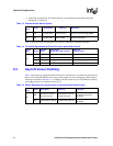
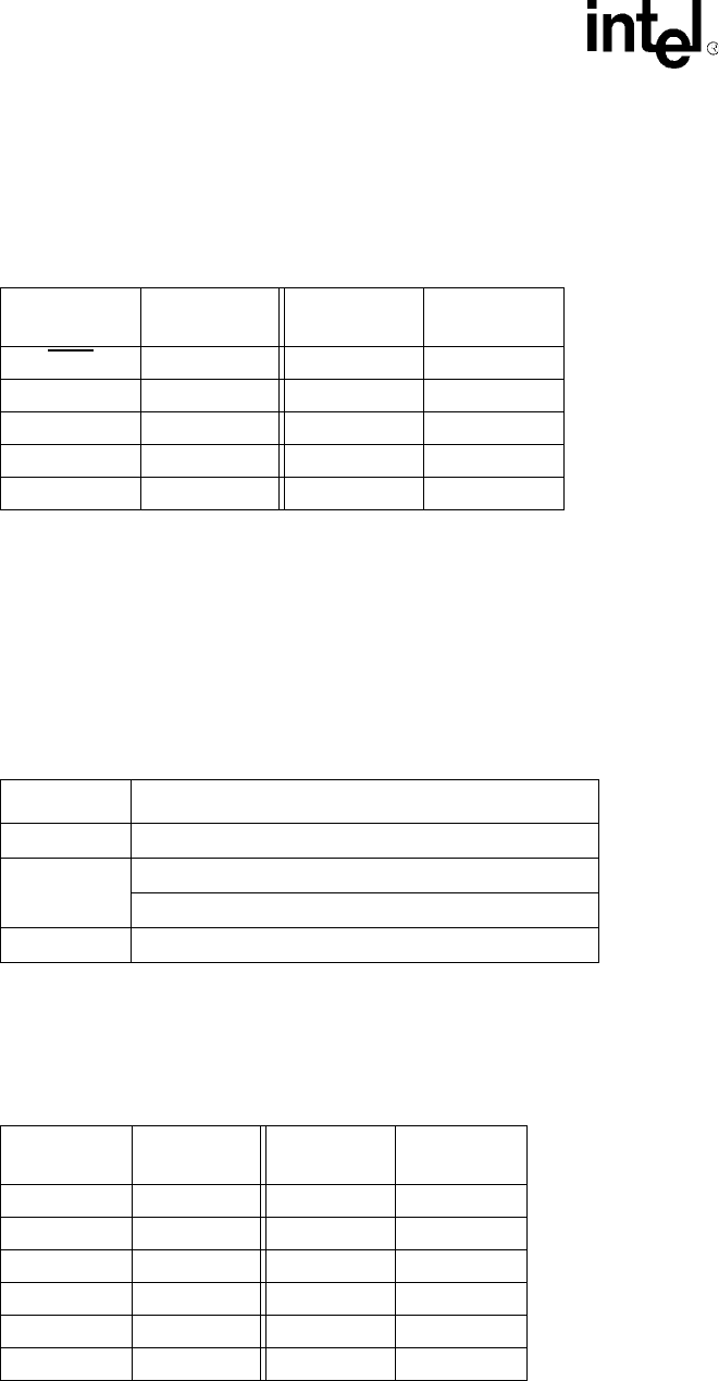
Table A-5 gives the pin assignments between the DE1B55503 schematic and the ten-pin JTAG
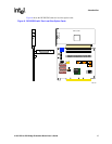
connector. See Figure 1 on page 6 for the location of this connector.
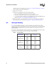
A.3 Factory Default Switch and Jumper Configuration
The DE1B55503 is configured at the factory for normal or typical operation.
• J8, the stake pin jumper, is not installed
• Table A-6 gives the factory configuration for the switch pack switches.
• Table A-7 gives the configuration of the zero-ohm resistor jumpers.
Table A-5. J1 JATAG Connector
Schematic
Number
Mictor
Pin Number
Mictor
Pin Number
Schematic
Number
TRST
12GND
TDI 3 4 GND
TD0 5 6 GND
TMS 7 8 GND
TCK 9 10 GND
Table A-6. Switch Pack Factory Defaults
Switches on Are set at the Factory.
a
a. The UP position leaves the switch lever pointing towards the
local option sockets.
J9 all switches are in the up position.
J20
SW1, SW2, and SW4 are n the up position
SW3 and SW5 are down.
J21 all switches are in the up position.
Table A-7. Resistor Jumper Factory Defaults
Resistor
Jumper
In/Out
Resistor
Jumper
In/Out
R65 IN R92 OUT
R68 OUT R93 OUT
R69 OUT R95 OUT
R72 IN R97 IN
R73 IN R115 IN
R91 IN R116 OUT


