6 21555 PCI-to-PCI Bridge Evaluation Board User’s Guide
Introduction
1.3 Major Components
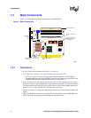
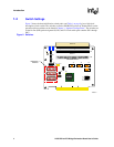
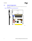
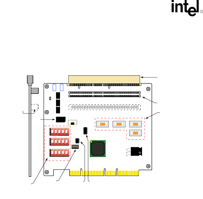
Figure 1 on page 6 shows the major components on the DE1B55503.
1.3.1 Connectors
• J1 is the 10-pin JTAG connector. See Table A-5 on page 26.
• J7 and J101 (slot 2 and slot 1) are local (secondary bus) PCI option slots.
— J101 (slot 1) can be used for a local processor with the insertion of a PCI Industrial
Computer Manufacturers Group
(PICMG) Single Board Computer. It is the PCI portion
of the PCI-ISA card edge connector. See Section 1.7 and Section 1.9.
• J102 (secondary bus) is the optional and connector-less slot. The optional slot is for a third
64-bit PCI connector. The through-holes are provided for installation of a local bus connector.
The default build for this board is for two option cards on the local bus. 66MHz operation is
limited to two (2) loads on the PCI bus. All connectors are 64-bit.
• The J2 and J4 Mictor* (scope pod) connectors provide test points for the all the 64-bit S_AD
signals.
• The J5 and J6 Mictor connectors are for other PCI control signals, such as C/BE, REQ, and
GNT. J6 provides test points for parallel ROM data and address lines.
Figure 1. Major Components
A8408-01
J1
J8
E4
J9
J20
J21
E9
E8
E7
E5
OPTIONAL SLOT
OPTIONAL
SLOT
Parallel
ROM
Initialization
Switches
JTAG
Connector
Serial
ROM
Clock Buffer
Mictor Connectors for
logic analyzers and
oscilloscopes
PCI option and PICMG
slot
PCI option and slot
SLOT 1
Y1
E2
E3
J4 J6 J2
J5
E1
21555
1 2 3 4 5
1 2 3 4 5
1 2 3 4 5
J102
J101
J7
SLOT 2
1
2
L2
L1+


