20 21555 PCI-to-PCI Bridge Evaluation Board User’s Guide
Operations and Installation
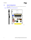
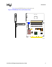
connectors and one (1) connector-less slot. Section 1.9, “Typical Configurations” on page 14
shows examples of typical PCI configurations.
6. Apply power to the system.
7. Verify the auto-configuration of the 21555 and other options.
a. If the on-board ROM is preloaded the 21555 banner displays.
b. Verify that system BIOS or firmware detects and configures the 21555.
c. To verify the loading of the SROM, run the MKSROM utility without an SROM file as an
input. See Section 2.3.1, “Programming the SROM” on page 18.
8. PCI bus data, address, and control signals are monitored by connecting a logic analyzer to
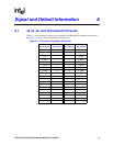
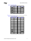
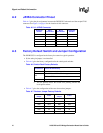
Mictor connectors J2, J4, J5, and J6. See Appendix A, “Signal and Default Information”
2.5 Interrupt Routing
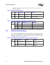
Table 9 shows the ORing of interrupts. A total of 12 interrupts are connected to each of three
secondary bus PCI slots but four interrupts are driven to the card edge. The 12 incoming interrupts
must be combined. Interrupt ORing is in accordance with the PCI-to-PCI Bridge Architecture
Specification V2.x.
In accordance with the PCI Bridge Architecture Specification, the interrupts of the devices on the
secondary slots are wire ORed and routed to PCI fingers of the DE1B55503.
Table 9. Interrupt ORing
Device Number
Interrupt Pin on
Device
Interrupt Pin on Board
Connector
5
(Optional Slot J101)
INTA#
INTB#
INTC#
INTD#
INTB#
INTC#
INTD#
INTA#
6
(PICMG slot J101)
INTA#
INTB#
INTC#
INTD#
INTA#
INTB#
INTC#
INTD#
7
(Top slot J7)
INTA#
INTB#
INTC#
INTD#
INTD#
INTA#
INTB#
INTC#


