


3-5
HARDWARE OVERVIEW
3
3.3.1 Flash (Program Memory)
Flash memory, as configured in the RISM monitor, is mapped to the upper 512 Kbytes of the
1 Mbyte 80x186 processor address space. The board includes a single 4 Mbit, 32-pin PSOP Flash
device at location U9 with 110 ns access time at 3.3 V and 60 ns access time at 5 V. This memory
runs with one wait state at 5 volts/20 MHz and 3.3 volts/16 MHz.
The device data bus can be configured to be either 8 or 16 bits wide (corresponding to the
80x188and the 80x186 processor, respectively). Jumper E5 determines the Flash bus width.
When E5 is in the A–B position, the bus is 8 bits wide; when E5 is in the B–C position, the bus
is 16 bits wide. The configurable bus width allows access to all 512 Kbytes of Flash memory.
If a user application requires nonvolatile memory for storage, Flash can be erased and written by
jumpering E3 for either 5 V or 12 V programming voltage (V
PP
) and using the proper
programming algorithm. The SmartVoltage* Flash device can be programmed using either
voltage. The Flash loader utility is located in the Flash boot block (upper 16 Kbytes, FC000h to
FFFFFh). Writes to this region are prohibited, regardless of the voltage on V
PP
, unless the RP#
input is at +12 volts or jumper E2 is set to unlock the boot block. Jumper E4 controls the voltage
on RP#. When E4 is in the B–C position, the +12 volt supply is connected to RP#. When E4 is in
the A–B position, RP# is connected to the board reset signal.
CAUTION: To access boot block memory, E4 must be in the B–C position and Port Pin 1.1
must be programmed to a logic 0 (enabling +12 volts). Accessing the boot block is
not recommended, as the Flash loader utility code could be corrupted.
3.3.1.1 Setting Up the Board for Flash Downloading
You can use the Flash utility host program, FLASHLDR.EXE, provided in the kit to download
your application program to the Flash memory. Upon reset or power-up, the Flash loader reads
port pin to determine whether to execute a loaded program, such as RISM, or download new
software to Flash memory.
To set up the board for Flash downloading:
1. Power-off the evaluation board and disconnect the serial cable from the PC.
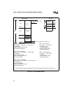
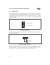
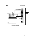
2. Port pin P2.6 on the secondary header (JP2) controls which programs execute at start-up.
Connect P2.6 to the +5 volt pin with jumper wire and 10 kΩ resistor. Figure 3-2 illustrates
this connection.
CAUTION: A 10 kΩ resistor is required when jumpering from the P2.6 pin to the 5 volt pin; if
this configuration is not used, the processor’s port control hardware could be
damaged.