


3-9
HARDWARE OVERVIEW
3
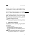
The Maxim MAX734 located at U11 is also a current-mode DC-DC converter. This device steps
up the V
CC
voltage to +12.0 volts. This voltage output is supplied to provide a V
PP
option for
Flash memory programming. The SHDN# input (pin 1) connects to a port pin (P1.1) on the
processor through an inverter. At reset, SHDN# is driven low to disable the +12 volt signal. The
output remains disabled until Port Pin 1.1 is programmed to a logic 0. When SHDN# is low, the
output (pin 8) is V
CC
minus a diode drop. The evaluation board uses SmartVoltage Flash. To
prevent unintentional writes to Flash, set jumpers E2 and E3 as indicated in Table 3-1.
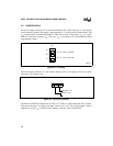
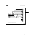
3.6 SERIAL INTERFACE
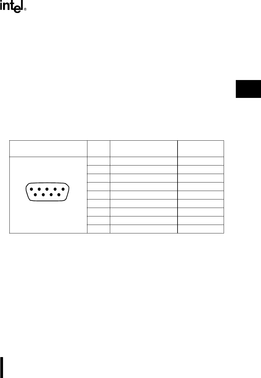
Connector P1 connects to your PC’s serial port. P1 interfaces pin-to-pin with a standard nine-pin
RS-232 serial connector. Verify that the cable being used provides all signals required.
Connector P2 is an additional serial port for user applications. Receive, Transmit, and Clear-to-
Send are connected. Other connector pins are routed to test points on the board.
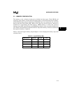
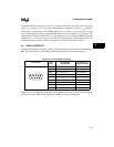
Table 3-3. P1 Host Serial Connector
P1 Connector
Pin
Nos.
Host RS-232
Signal Name
Connection on
Evaluation Board
1 (CF) DCD Data Carrier Detect DTR P1-pin 4
2 (BB) RxD Receive Data TxD of MAX561
3 (BA) TxD Transmit Data RxD of MAX561
4 (CD) DTR Data Terminal Ready INIT
5 (AB) SG Signal Ground Digital Ground
6 (CC) DSR Data Set Ready DTR P1-pin4
7 (CA) RTS Request To Send CTS P1-pin8
8 (CB) CTS Clear To Send RTS P1-pin7
9 (CE) RI Ring Indicator Run Indicator
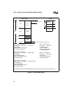
1234 5
6
78
9