


10 PRELIMINARY
8XC251SA/SB/SP/SQ HIGH-PERFORMANCE CHMOS MICROCONTROLLER
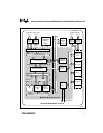
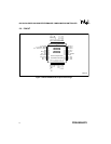
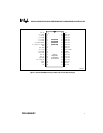
3.0 SIGNALS
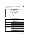
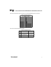
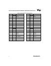
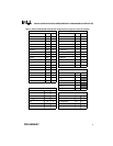
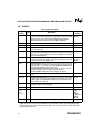
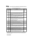
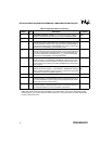
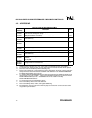
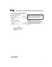
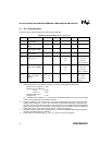
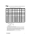
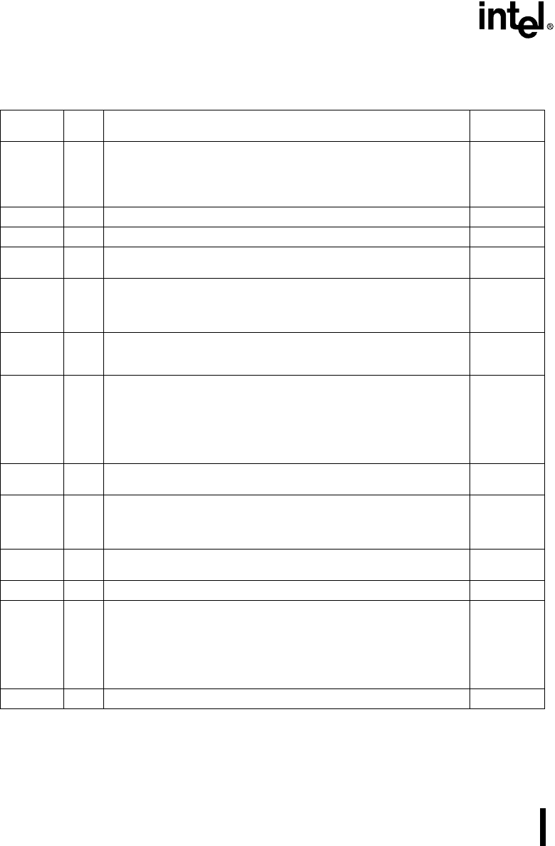
Table 6. Signal Descriptions
Signal
Name
Type Description
Alternate
Function
A17 O 18th Address Bit (A17). Output to memory as 18th external address
bit (A17) in extended bus applications, depending on the values of bits
RD0 and RD1 in configuration byte UCONFIG0 (see Chapter 4,
“Device Configuration,” of the 8XC251SA/SB/SP/SQ Embedded
Microcontroller User’s Manual). See also RD# and PSEN#.
P1.7/CEX4/
WCLK
A16 O Address Line 16. See RD#. RD#
A15:8
†
O Address Lines. Upper address lines for the external bus. P2.7:0
AD7:0
†
I/O Address/Data Lines. Multiplexed lower address lines and data lines
for external memory.
P0.7:0
ALE O Address Latch Enable. ALE signals the start of an external bus cycle
and indicates that valid address information is available on lines A15:8
and AD7:0. An external latch can use ALE to demultiplex the address
from the address/data bus.
PROG#
CEX4:0 I/O Programmable Counter Array (PCA) Input/Output Pins. These are
input signals for the PCA capture mode and output signals for the PCA
compare mode and PCA PWM mode.
P1.6:3
P1.7/A17/
WAIT#
EA# I External Access. Directs program memory accesses to on-chip or off-
chip code memory. For EA# = 0, all program memory accesses are off-
chip. For EA# = 1, an access is to on-chip ROM/OTPROM/EPROM if
the address is within the range of the on-chip
ROM/OTPROM/EPROM; otherwise the access is off-chip. The value
of EA# is latched at reset. For devices without on-chip
ROM/OTPROM/EPROM, EA# must be strapped to ground.
V
PP
ECI I PCA External Clock Input. External clock input to the 16-bit PCA
timer.
P1.2
INT1:0# I External Interrupts 0 and 1. These inputs set bits IE1:0 in the TCON
register. If bits IT1:0 in the TCON register are set, bits IE1:0 are set by
a falling edge on INT1#/INT0#. If bits INT1:0 are clear, bits IE1:0 are
set by a low level on INT1:0#.
P3.3:2
PROG# I Programming Pulse. The programming pulse is applied to this pin for
programming the on-chip OTPROM.
ALE
P0.7:0 I/O Port 0. This is an 8-bit, open-drain, bidirectional I/O port. AD7:0
P1.0
P1.1
P1.2
P1.7:3
I/O Port 1. This is an 8-bit, bidirectional I/O port with internal pullups. T2
T2EX
ECI
CEX3:0
CEX4/A17/
WAIT#/
WCLK
P2.7:0 I/O Port 2. This is an 8-bit, bidirectional I/O port with internal pullups. A15:8
†
The descriptions of A15:8/P2.7:0 and AD7:0/P0.7:0 are for the nonpage-mode chip configuration (com-
patible with 44-pin PLCC and 40-pin DIP MCS 51 microcontrollers). If the chip is configured for page-
mode operation, port 0 carries the lower address bits (A7:0), and port 2 carries the upper address bits
(A15:8) and the data (D7:0).