


16 PRELIMINARY
8XC251SA/SB/SP/SQ HIGH-PERFORMANCE CHMOS MICROCONTROLLER
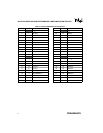
5.1 D.C. Characteristics
Parameter values apply to all devices unless otherwise indicated.
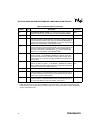
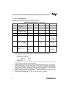
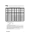
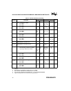
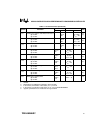
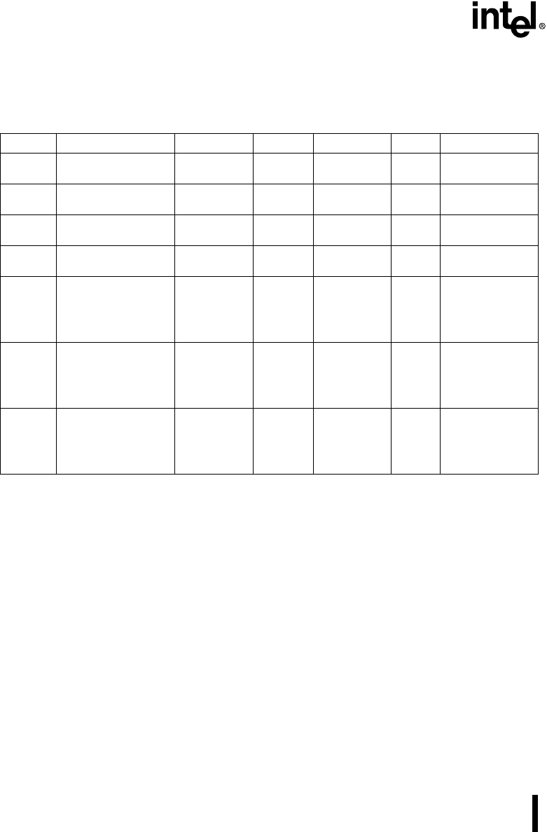
Table 9. DC Characteristics at V
CC
= 4.5 – 5.5 V
Symbol Parameter Min Typical Max Units Test Conditions
V
IL
Input Low Voltage
(except EA#)
-0.5 0.2V
CC
– 0.1 V
V
IL1
Input Low Voltage
(EA#)
0 0.2V
CC
– 0.3 V
V
IH
Input High Voltage
(except XTAL1, RST)
0.2V
CC
+ 0.9 V
CC
+ 0.5 V
V
IH1
Input High Voltage
(XTAL1, RST)
0.7V
CC
V
CC
+ 0.5 V
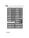
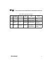
V
OL
Output Low Voltage
(Port 1, 2, 3)
0.3
0.45
1.0
VI
OL
= 100 µA
I
OL
= 1.6 mA
I
OL
= 3.5 mA
(Note 1, Note 2)
V
OL1
Output Low Voltage
(Port 0, ALE, PSEN#)
0.3
0.45
1.0
VI
OL
= 200 µA
I
OL
= 3.2 mA
I
OL
= 7.0 mA
(Note 1, Note 2)
V
OH
Output High Voltage
(Port 1, 2, 3, ALE,
PSEN#)
V
CC
– 0.3
V
CC
– 0.7
V
CC
– 1.5
VI
OH
= -10 µA
I
OH
= -30 µA
I
OH
= -60 µA
(Note 3)
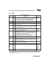
NOTES:
1. Under steady-state (non-transient) conditions, I
OL
must be externally limited as follows:
Maximum I
OL
per port pin: 10 mA
Maximum I
OL
per 8-bit port:
port 0 26 mA
ports 1–3 15 mA
Maximum Total I
OL
for
all output pins 71 mA
If I
OL
exceeds the test conditions, V
OL
may exceed the related specification. Pins are not guaranteed
to sink current greater than the listed test conditions.
2. Capacitive loading on ports 0 and 2 may cause spurious noise pulses above 0.4 V on the low-level
outputs of ALE and ports 1, 2, and 3. The noise is due to external bus capacitance discharging into
the port 0 and port 2 pins when these pins change from high to low. In applications where capacitive
loading exceeds 100 pF, the noise pulses on these signals may exceed 0.8 V. It may be desirable to
qualify ALE or other signals with a Schmitt trigger or CMOS-level input logic.
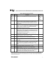
3. Capacitive loading on ports 0 and 2 causes the V
OH
on ALE and PSEN# to drop below the specifica-
tion when the address lines are stabilizing.
4. Typical values are obtained using V
CC
= 5.0, T
A
= 25°C and are not guaranteed.