


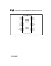

PRELIMINARY 11
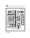
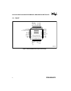
8XC251SA/SB/SP/SQ HIGH-PERFORMANCE CHMOS MICROCONTROLLER
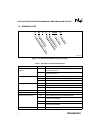
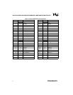
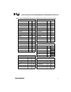
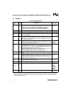
P3.0
P3.1
P3.3:2
P3.5:4
P3.6
P3.7
I/O Port 3. This is an 8-bit, bidirectional I/O port with internal pullups. RXD
TXD
INT1:0#
T1:0
WR#
RD#/A16
PSEN# O Program Store Enable. Read signal output. This output is asserted
for a memory address range that depends on bits RD0 and RD1 in
configuration byte UCONFIG0 (see RD# and Chapter 4, “Device Con-
figuration,” in the 8XC251SA/SB/SP/SQ Embedded Microcontroller
User’s Manual).
—
RD# O Read or 17th Address Bit (A16). Read signal output to external data
memory or 17th external address bit (A16), depending on the values of
bits RD0 and RD1 in configuration byte UCONFIG0. (See PSEN# and
Chapter 4, “Device Configuration,” in the 8XC251SA/SB/SP/SQ
Embedded Microcontroller User’s Manual).
P3.7/A16
RST I Reset. Reset input to the chip. Holding this pin high for 64 oscillator
periods while the oscillator is running resets the device. The port pins
are driven to their reset conditions when a voltage greater than V
IH1
is
applied, whether or not the oscillator is running. This pin has an inter-
nal pulldown resistor, which allows the device to be reset by connect-
ing a capacitor between this pin and V
CC
.
Asserting RST when the chip is in idle mode or powerdown mode
returns the chip to normal operation.
—
RXD I/O Receive Serial Data. RXD sends and receives data in serial I/O mode
0 and receives data in serial I/O modes 1, 2, and 3.
P3.0
T1:0 I Timer 1:0 External Clock Inputs. When timer 1:0 operates as a
counter, a falling edge on the T1:0 pin increments the count.
P3.5:4
T2 I/O Timer 2 Clock Input/Output. For the timer 2 capture mode, this signal
is the external clock input. For the clock-out mode, it is the timer 2
clock output.
P1.0
T2EX I Timer 2 External Input. In timer 2 capture mode, a falling edge ini-
tiates a capture of the timer 2 registers. In auto-reload mode, a falling
edge causes the timer 2 registers to be reloaded. In the up-down
counter mode, this signal determines the count direction: 1 = up, 0 =
down.
P1.1
TXD O Transmit Serial Data. TXD outputs the shift clock in serial I/O mode 0
and transmits serial data in serial I/O modes 1, 2, and 3.
P3.1
V
CC
PWR Supply Voltage. Connect this pin to the +5V supply voltage. —
V
CC2
PWR Secondary Supply Voltage 2. This supply voltage connection is pro-
vided to reduce power supply noise. Connection of this pin to the +5V
supply voltage is recommended. However, when using the 8XC251SB
as a pin-for-pin replacement for the 8XC51FX, V
SS2
can be uncon-
nected without loss of compatibility. (Not available on DIP)
—
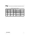
Table 6. Signal Descriptions (Continued)
Signal
Name
Type Description
Alternate
Function
†
The descriptions of A15:8/P2.7:0 and AD7:0/P0.7:0 are for the nonpage-mode chip configuration (com-
patible with 44-pin PLCC and 40-pin DIP MCS 51 microcontrollers). If the chip is configured for page-
mode operation, port 0 carries the lower address bits (A7:0), and port 2 carries the upper address bits
(A15:8) and the data (D7:0).