


PRELIMINARY 21
8XC251SA/SB/SP/SQ HIGH-PERFORMANCE CHMOS MICROCONTROLLER
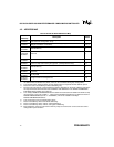
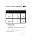
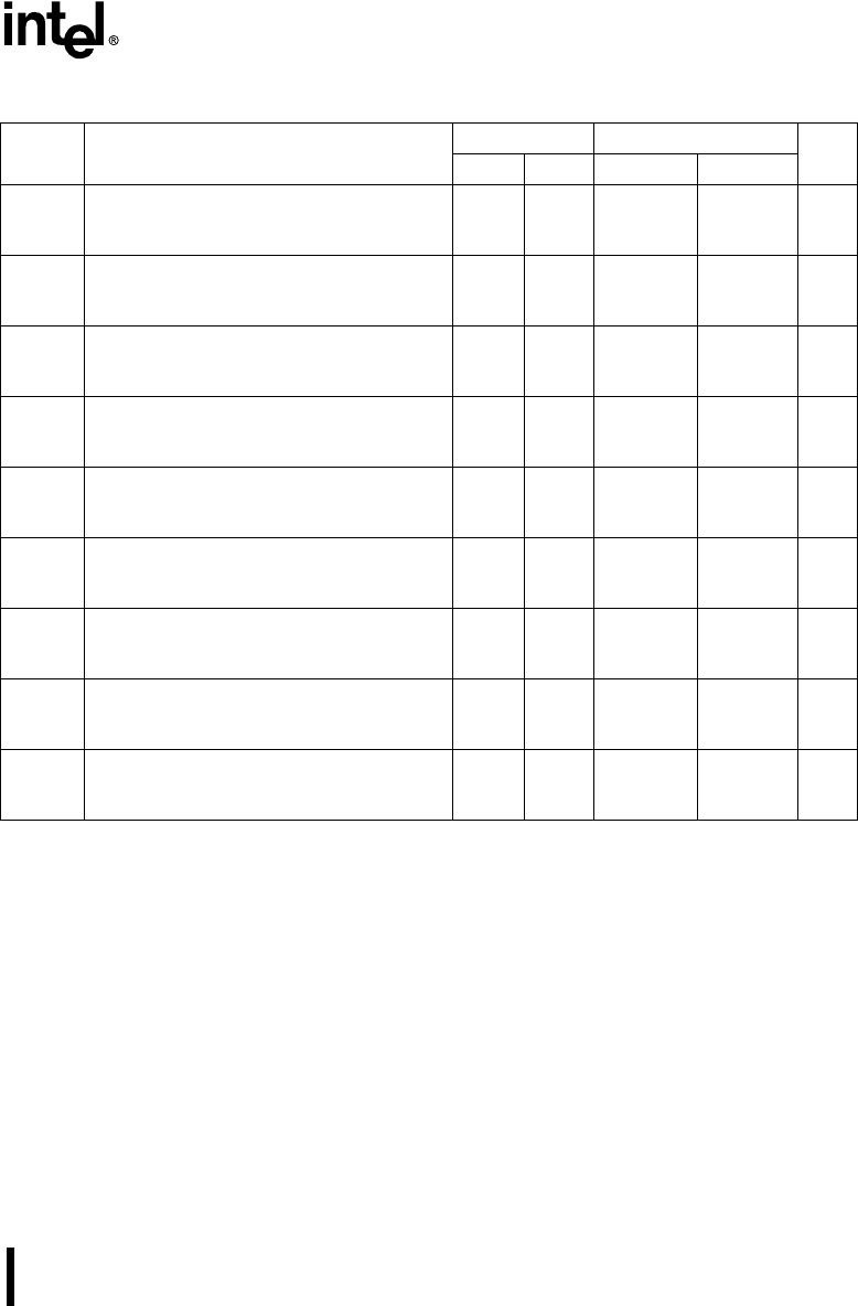
T
AVDV1
Address (P0) Valid to Valid Data/Instruction In
@ 12 MHz
@ 16 MHz
243.2
160
4(1+M/2)
T
OSC
– 90
ns
(3)
T
AVDV2
Address (P2) Valid to Valid Data/Instruction In
@ 12 MHz
@ 16 MHz
268.2
185
4(1+M/2)
T
OSC
– 65
ns
(3)
T
AVDV3
Address (P0) Valid to Valid Instruction In
@ 12 MHz
@ 16 MHz
116.6
75
2T
OSC
– 50
ns
T
AVRL
(2) Address Valid to RD#/PSEN# Low
@ 12 MHz
@ 16 MHz
121.6
80
2(1+M)
T
OSC
– 45
ns
(3)
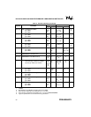
T
AVWL1
Address (P0) Valid to WR# Low
@ 12 MHz
@ 16 MHz
126.6
85
2(1+M)
T
OSC
– 40
ns
(3)
T
AVWL2
Address (P2) Valid to WR# Low
@ 12 MHz
@ 16 MHz
146.6
105
2(1+M)
T
OSC
– 20
ns
(3)
T
WHQX
Data Hold after WR# High
@ 12 MHz
@ 16 MHz
63.3
42.5
T
OSC
– 20
ns
T
QVWH
Data Valid to WR# High
@ 12 MHz
@ 16 MHz
138.6
97
2(1+N)
T
OSC
– 28
ns
(4)
T
WHAX
WR# High to Address Hold
@ 12 MHz
@ 16 MHz
156.6
115
2T
OSC
– 10
ns
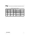
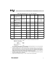
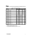
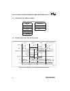
Table 11. AC Characteristics (Continued)
Symbol Parameter
@ Max F
osc
(1) F
osc
Variable
Units
Min Max Min Max
NOTES:
1. 16 MHz.
2. Specifications for PSEN# are identical to those for RD#.
3. In the formula, M=Number of wait states (0 or 1) for ALE.
4. In the formula, N=Number of wait states (0,1,2, or 3) for RD#/PSEN#/WR#.
5. “Typical” specifications are untested and not guaranteed.