


PRELIMINARY 19
8XC251SA/SB/SP/SQ HIGH-PERFORMANCE CHMOS MICROCONTROLLER
5.2 Definition of AC Symbols
5.3 A.C. Characteristics
Test Conditions: Capacitive load on all pins = 50 pF.
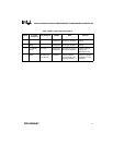
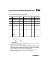
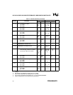
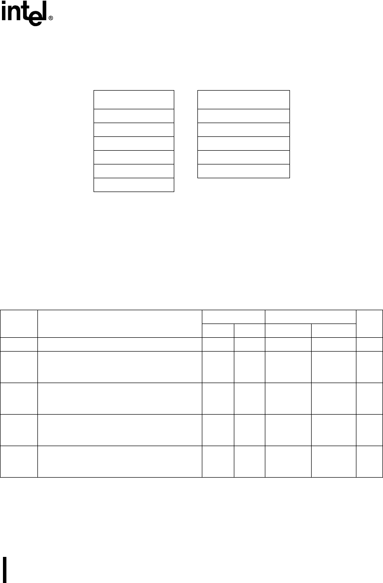
Table 10. AC Timing Symbol Definitions
Signals Conditions
A Address H High
D Data In L Low
L ALE V Valid
Q Data Out X No Longer Valid
R RD#/PSEN# Z Floating
W WR#
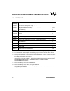
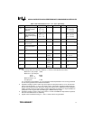
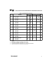
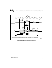
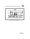
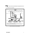
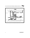
Table 11 lists AC timing parameters for the
8XC251SA/SB/SP/SQ with no wait states. External
wait states can be added by extending
PSEN#/RD#/WR# and/or by extending ALE. In the
table, Notes 3 and 5 mark parameters affected by an
ALE wait state, and Notes 4 and 5 mark parameters
affected by a PSEN#/RD#/WR# wait state.
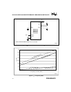
Figures 8–10 show the bus cycles with the timing
parameters.
Table 11. AC Characteristics
Symbol Parameter
@ Max F
osc
(1) F
osc
Variable
Units
Min Max Min Max
F
OSC
XTAL1 Frequency N/A N/A 0 16 MHz
T
OSC
1/F
OSC
@ 12 MHz
@ 16 MHz
N/A N/A
83.3
62.5
ns
T
LHLL
ALE Pulse Width
@ 12 MHz
@ 16 MHz
73.3
52.5
(1+2M)
T
OSC
– 10
ns
(3)
T
AVLL
Address Valid to ALE Low
@ 12 MHz
@ 16 MHz
58.3
37.5
(1+2M)
T
OSC
– 25
ns
(3)
T
LLAX
Address Hold after ALE Low
@ 12 MHz
@ 16 MHz
15
15 15
ns
NOTES:
1. 16 MHz.
2. Specifications for PSEN# are identical to those for RD#.
3. In the formula, M=Number of wait states (0 or 1) for ALE.
4. In the formula, N=Number of wait states (0,1,2, or 3) for RD#/PSEN#/WR#.
5. “Typical” specifications are untested and not guaranteed.