


ECB-865
ECB-865 User’s Manual 45
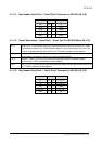
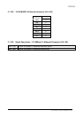
3.11.38 Signal Description – Proprietary PCI Connector (J21)
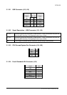
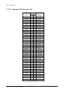
3.11.38.1 Address & Data
AD [31::00]
Address and Data are multiplexed on the same PCI pins. A bus transaction consists
of an address phase followed by one or more data phases. PCI supports both read
and write bursts.
The address phase is the clock cycle in which FRAME# is asserted. During the
address phase AD [31::00] contain a physical address (32 bits). For I/O, this is a
byte address; for configuration and memory, it is a DWORD address. During data
phases AD [07::00] contain the least significant byte (lsb) and AD [31::24] contain
the most significant byte (msb). Write data is stable and valid when IRDY# is
asserted and read data is stable and valid when TRDY# is asserted. Data is
transferred during those clocks where both IRDY# and TRDY# are asserted.
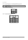
C/BE [3::0]#
Bus Command and Byte Enables are multiplexed on the same PCI pins. During the
address phase of a transaction, C/BE [3::0]# define the bus command. During the
data phase C/BE [3::0]# are used as Byte Enables. The Byte Enables are valid for
the entire data phase and determine which byte lanes carry meaningful data.
C/BE[0]# applies to byte 0 (lsb) and C/BE[3]# applies to byte 3 (msb).
PAR
Parity is even parity across AD [31::00] and C/BE [3::0]#. Parity generation is
required by all PCI agents. PAR is stable and valid one clock after the address
phase. For data phases, PAR is stable and valid one clock after either IRDY# is
asserted on a write transaction or TRDY# is asserted on a read transaction. Once
PAR is valid, it remains valid until one clock after the completion of the current data
phase. (PAR has the same timing as AD[31::00], but it is delayed by one clock.) The
master drives PAR for address and write data phases; the target drives PAR for read
data phases.