IA-32 Intel® Architecture Optimization
1-20
Levels in the cache hierarchy are not inclusive. The fact that a line is in
level i does not imply that it is also in level i+1. All caches use a
pseudo-LRU (least recently used) replacement algorithm.
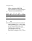
Table 1-1 provides parameters for all cache levels for Pentium and Intel
Xeon Processors with CPUID model encoding equals 0, 1, 2 or 3.
1
Each read due to a cache miss fetches a sector, consisting of two adjacent cache lines; a write operation is 64 bytes.
2
Pentium 4 and Intel Xeon processors with CPUID model encoding value of 2 have a second level cache of 512 KB.
On processors without a third level cache, the second-level cache miss
initiates a transaction across the system bus interface to the memory
sub-system. On processors with a third level cache, the third-level cache
miss initiates a transaction across the system bus. A bus write
transaction writes 64 bytes to cacheable memory, or separate 8-byte
chunks if the destination is not cacheable. A bus read transaction from
cacheable memory fetches two cache lines of data.
The system bus interface supports using a scalable bus clock and
achieves an effective speed that quadruples the speed of the scalable bus
clock. It takes on the order of 12 processor cycles to get to the bus and
Table 1-1 Pentium 4 and Intel Xeon Processor Cache Parameters
Level (Model) Capacity
Associa-
tivity
(ways)
Line Size
(bytes)
Access Latency,
Integer/
floating-point
(clocks)
Write Update
Policy
First (Model 0,
1, 2)
8 KB 4 64 2/9 write through
First (Model 3) 16 KB 8 64 4/12 write through
TC (All models) 12K µops 8 N/A N/A N/A
Second (Model
0, 1, 2)
256 KB or 512
KB
2
864
1
7/7 write back
Second (Model
3, 4)
1 MB 8 64
1
18/18 write back
Second (Model
3, 4, 6)
2 MB 8 64
1
20/20 write back
Third (Model 0,
1, 2)
0, 512 KB, 1
MB or 2 MB
864
1
14/14 write back


