


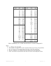
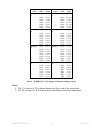
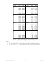
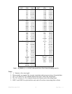

DDR3THIN-MN-XXX 47 Doc. Rev. 1.11
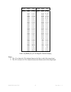
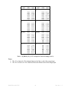
Group
Name
Signal
Name
TLA
Input
Group
Name
Signal
Name
TLA
Input
CheckBit
s
CB7 M_A1:5 DataMasks DM7 S_A2:4
CB6 M_A1:4 DM6 S_A3:6
CB5 M_A1:0 DM5 S_A1:0
CB4 M_A0:7 DM4 M_C2:0
CB3 M_A1:6 DM3 M_A0:2
CB2 M_A1:3 DM2 S_CK3
CB1 M_CK1 DM1 S_E3:5
CB0 M_A0:5 DM0 S_E2:6
Strobes
2
DQS8 M_A1:2 Address
2
BA2 M_A3:0
DQS7 S_A2:6 BA1 M_C3:7
DQS6 S_A3:5 BA0 M_C1:6
DQS5 S_CK1 A15 M_CK0
DQS4 M_C2:3 A14 M_A2:5
DQS3 M_A0:0 A13 M_CK3
DQS2 S_C3:0 A12/BC# M_A2:4
DQS1 S_E3:6 A11 M_A2:6
DQS0 S_E2:4 A10/AP M_C1:3
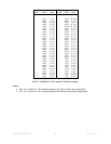
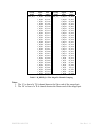
Control
2
CKE1 M_A3:2 A9 M_A2:1
CKE0 M_A3:1 A8 M_A2:0
S3# M_C2:5 A7 M_A2:3
S2# M_C3:0 A6 M_C0:2
S1# M_C3:4 A5 M_A2:2
S0# M_C3:3 A4 M_C0:5
BA2 M_A3:0 A3 M_C1:0
BA1 M_C3:7 A2 M_Q1
BA0 M_C1:6 A1 M_C1:1
A15
M_CK0 A0 M_C1:5
A14 M_A2:5 Orphans PAR_IN M_C1:2
A13 M_CK3 ERR_OUT# M_A2:7
A12/BC# M_A2:4 TEST M_A3:7
A10/AP M_C1:3 RESET# M_A3:6
RAS# M_C3:6 ODT1 M_C3:1
CAS# M_C3:5 ODT0 M_C3:2
WE# M_C1:7 Misc
2,5
MISC1 M_A3:5
MISC0 M_A3:4
DDRCK0 M_C1:4
Table 4 – B_DDR3D_2D/_2G (<=1333MT/s Read and Write) TLA Channel Grouping (cont’d.)
Notes:
1. ‘ # ‘ denotes a low-true signal
2. These signals are required for accurate acquisition and post-processing of acquired data
3. The ‘S’ in front of a TLA channel denotes the Slave card of the merged pair
4. The ‘M’ in front of a TLA channel denotes the Master card of the merged pair
5. MISC1 and MISC0 are placeholders only and will not have interesting data on them