


DDR3THIN-MN-XXX 53 Doc. Rev. 1.11
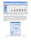
5.3 Adjusting Input Thresholds for Proper Data Acquisition
The Interposer DDR3 support was designed to work with the new Nexus Low Profile Distributed
probes. To maximize the electrical characteristics of the acquired waveforms the probe input
resistors values were placed at 510 ohms. This value results in a divide by ten of the signals to
the logic analyzer when using the NEX-PRB1X-T and NEX-PRB2X-T probes. The logic
analyzer expects a divide by 20. Since the divide value is different than the standard Tektronix
probe the voltage swing and offset will be higher than expected, and the thresholds will be
different. Instead of the expected 0.75 threshold of approximately 1.9V threshold will be
required. Use of the logic analyzer output to a scope will be required to determine the exact
threshold for the system under test.
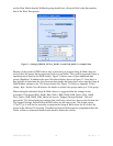
5.4 DDR3 and DDR3SPA
It is strongly recommended that Nexus’ DDR3SPA (DDR3 Sample Point Analyzer) be used to
determine the proper sample point setting necessary for accurate Read and Write data
acquisition. Given the correct DDR bus parameters (Latency, Burst Length, etc.) SPA will
analyze any Read and/or Write bus transactions in MagniVu memory and return suggested
sample points. Refer to the DDR SPA documentation for more specific information on using this
software.
If for whatever reason DDR3SPA doesn’t appear to provide good sample point setting
information the following sections describe how to evaluate acquired DDR3 data to determine
the proper sample points manually.
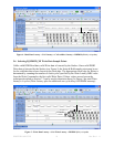
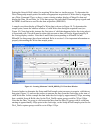
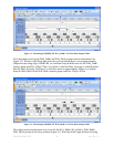
5.5 Selecting B_DDR3E_XX Read Data Sample Points
For the DDR3 Read data to be properly acquired it is necessary to choose the proper sample
points to ensure that data is acquired at the proper point in the transaction. Since valid DDR3
Read data is straddled by the Strobes (see Figure 4) the Setup & Hold sample point must be set
for the valid data that occurs closest to the clock edge. The appropriate clock edge for Reads is
determined by adding the Additive Latency value to the CAS Latency value and adding one if
Registered memory (RDIMMs) are being used, resulting in the total number of clock cycles from
the Read Command to the first valid Read Data. (If these values are not known the technique
described in Section 7.3 can be used to determine the necessary values with the exception of
whether or not the memory is RDIMM or UDIMM.) In Figure 4 the total Read latency is 6
cycles.
The B_DDR3D_XX supports acquire two samples of valid Read data on each rising edge of the
DDR3 clock. So to acquire both pieces of data the RdA_DatHi/Lo data groups must have their
sample point set to that shown by Sample Pt. #1 in the Figure, and the RdB_DatHi/Lo data
groups must have their sample point set to that shown by Sample Pt. #2.