


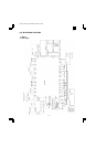
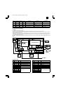
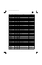
Pin No. Pin name Signal name I/O Function Purpose Descriptions
124 MD1 — IN Operation mode setting pin 1 Operation mode setting
(MODE 4)
Operation mode 4
125 MD2 — IN Operation mode setting pin 2 Operation mode setting
(MODE 4)
Operation mode 4
126 PG0 RY/BY IN General port G0 Flash ROM busy signal 0: Busy state
127 /CS3 /CS3 OUT Area 3 chip select I/O extension ASIC chip select L: Select effective
128 /CS2 /CS2 OUT Area 2 chip select Image ASIC chip select L: Select effective
(Pin descriptions) IN: Input pin OUT: Output pin BIDIR: Bi-directional pin ODN: Open drain output pin TR1: 3-state output pin POW: Power pin
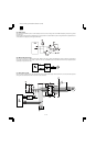
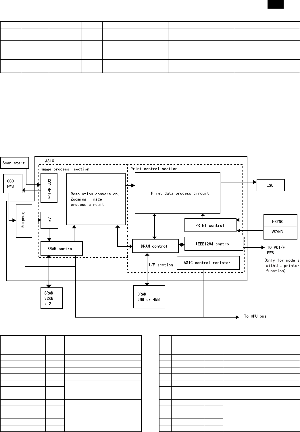
(3) Image ASIC (HG73C039FD)
a. Outline
Fig. 4 shows the block diagram of the ASIC.
The ASIC is composed of the following three blocks; the image process section, the print control section, and the I/F section.
The image process section processes the image data from the CCD PWB according to the operation mode, such as shading, AE process,
resolution conversion. and zooming.
The print control section outputs the image-processed data during copying to the LSU (Laser unit) in synchronization with writing timing of the LSU.
The I/F section controls communication of interface (IEEE1284) with the host PC and controls DRAM of send/receive data buffer with the host PC.
(Only for models with the printer function)
The ASIC is controlled by the CPU which writes the operation mode and the set values necessary for each operation mode to the ASIC control
register.
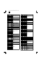
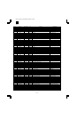
b. pin/signal table
PIN
No.
Signal name IN/OUT Description
1 /SCANSP IN Scanner process interrupt signal
2 /PRSTART IN Print start trigger signal
3 TMON IN Toner motor ON/OFF
4 TMCLK IN Toner motor reference clock
5 3.3V Power
6 CPUAD7 IN
CPU address bus
7 CPUAD6 IN
8 GND Power
9 CPUAD5 IN
CPU address bus
10 CPUAD4 IN
11 CPUAD3 IN
12 CPUAD2 IN
13 CPUAD1 IN
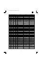
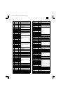
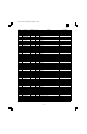
PIN
No.
Signal name IN/OUT Description
14 /CPUSYNC OUT Horizontal synchronization signal
15 /INTR OUT Interruption request signal
16 /CPUCS IN CPU chip select signal
17 /RESET IN Reset signal
18 5V Power
19 GND Power
20 3.3V Power
21 GND Power
22 MDATA15 IN/OUT
Data bus of DRAM (page memory)
23 MDATA14 IN/OUT
24 MDATA13 IN/OUT
25 MDATA12 IN/OUT
26 MDATA11 IN/OUT
AR-161
AR-160/161 FM/E [13] ELECTRICAL SECTION 12/1/1998
13 – 5