


SSI
EPS2U Power Supply Design Guide, V2.1
9 MTBF............................................................................................................................................................ 30
10 Agency Requirements................................................................................................................................ 30
Figures
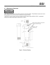
Figure 1: Enclosure Drawing .................................................................................................................................... 7
Figure 2: Output Voltage Timing............................................................................................................................. 22
Figure 3: Turn On/Off Timing (Single Power Supply)............................................................................................. 23
Figure 4: PSON# Signal Characteristics ................................................................................................................ 26
Tables
Table 1: Thermal Requirements............................................................................................................................... 8
Table 2: AC Input Rating .......................................................................................................................................... 9
Table 3: Efficiency .................................................................................................................................................... 9
Table 4: AC Line Sag Transient Performance........................................................................................................ 11
Table 5: AC Line Surge Transient Performance .................................................................................................... 11
Table 6: 12V Rail Summary.................................................................................................................................... 12
Table 7: P1 Baseboard Power Connector – Common Plane................................................................................. 13
Table 8: P1 Baseboard Power Connector – Split Plane......................................................................................... 13
Table 9: Processor Power Connector – Common Plane........................................................................................ 14
Table 10: Processor Power Connector – Split Plane ............................................................................................. 14
Table 11: Peripheral Power Connectors................................................................................................................. 15
Table 12: P9 Floppy Power Connector................................................................................................................... 15
Table 13: Server Signal Connector ........................................................................................................................ 16
Table 14: 480 W Load Ratings – Common Plane.................................................................................................. 17
Table 15: 550 W Load Ratings – Split Plane.......................................................................................................... 17
Table 16: 600 W Load Ratings – Split Plane.......................................................................................................... 18
Table 17: 650 W Load Ratings – Split Plane.......................................................................................................... 18
Table 18: Voltage Regulation Limits....................................................................................................................... 19
Table 19: Optional +5V Regulation Limits.............................................................................................................. 19
Table 20: Transient Load Requirements................................................................................................................ 20
Table 21: Capacitve Loading Conditions................................................................................................................ 20
Table 22: Ripple and Noise .................................................................................................................................... 21
Table 23: Output Voltage Timing............................................................................................................................ 21
Table 24: Turn On/Off Timing................................................................................................................................. 22
Table 25: Over Current Protection.......................................................................................................................... 24
Table 26: Over Current Protection.......................................................................................................................... 25
Table 27: Over Voltage Limits ................................................................................................................................ 25
Table 28: PSON
#
Signal Characteristic.................................................................................................................. 26
Table 29: PWOK Signal Characteristics................................................................................................................. 27
Table 30: FRU Device Information ......................................................................................................................... 28
Table 31: FRU Device Product Information Area................................................................................................... 28
Table 32: FRU Device Product Information Area................................................................................................... 29
- 4 -