MSP430x11x1
MIXED SIGNAL MICROCONTROLLER
SLAS241C – SEPTEMBER 1999 – REVISED JUNE 2000
14
POST OFFICE BOX 655303 • DALLAS, TEXAS 75265
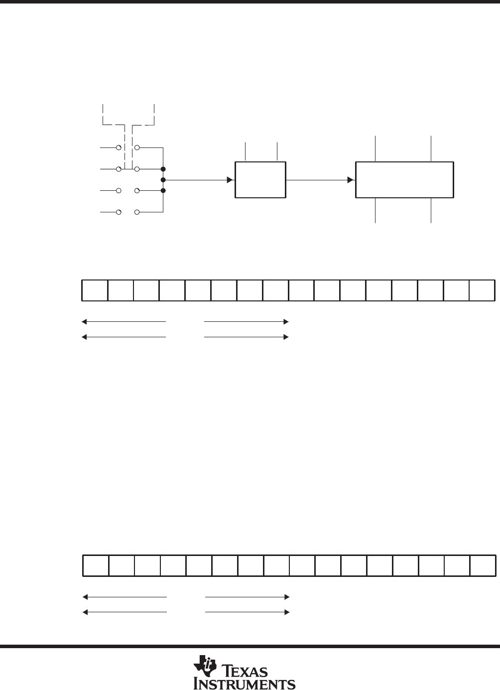
flash memory, timing generator, control register FCTL2 (continued)
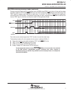
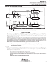
The flash timing generator is reset with PUC. It is also reset if the emergency exit bit EMEX is set.
Control register FCTL2 may not be written to if the BUSY bit is set; otherwise, an access violation will occur
(ACCVIFG=1).
Read access is possible at any time without restrictions.
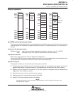
ACLK
0
1
2
3
SSEL1
MCLK
SMCLK
SMCLK
Divider,
1 .. 64
Reset
Flash Timing
Generator
SSEL0
FN5.......... FN0
f
X
PUC EMEX
BUSY WAIT
Write ’1’ to
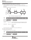
Figure 1. Flash Memory Timing Generator Diagram
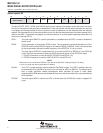
FCTL2
012Ah
FN2 FN1 FN0
0
rw-0rw-1rw–0
7
rw–0
SSEL0
rw–1
FN5 FN4 FN3
15
FCTL2 read:
096h
FCTL2 write:
0A5h
rw-0rw-0rw-0
8
SSEL1
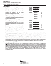
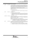
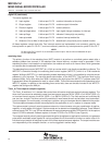
The control bits are:
FN0–FN5 012Ah, bit0–5 These six bits define the division rate of the clock signal. The division
rate is 1 to 64, according to the digital value of FN5 to FN0 plus one.
SSEL0, SSEL1 012Ah, bit6,7 Clock source select
0: ACLK
1: MCLK
2: SMCLK
3: SMCLK
The flash timing generator is reset with PUC. It is also reset if the EMEX bit is set.
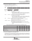
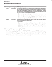
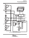
flash memory control register FCTL3
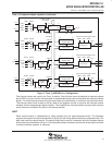
There are no restrictions to modify this control register.
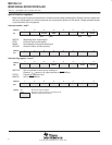
FCTL3
012Ch
KEYV BUSY
0
r(w)-0rw-(0)rw–0
7
r0
res.
r0
EMEX Lock WAIT
15
FCTL3 read:
096h
FCTL3 write:
0A5h
rw-1rw-1rw-0
8
ACCV
IFG
res.


