


MSP430x11x1
MIXED SIGNAL MICROCONTROLLER
SLAS241C – SEPTEMBER 1999 – REVISED JUNE 2000
29
POST OFFICE BOX 655303 • DALLAS, TEXAS 75265
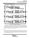
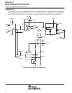
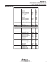
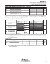
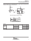
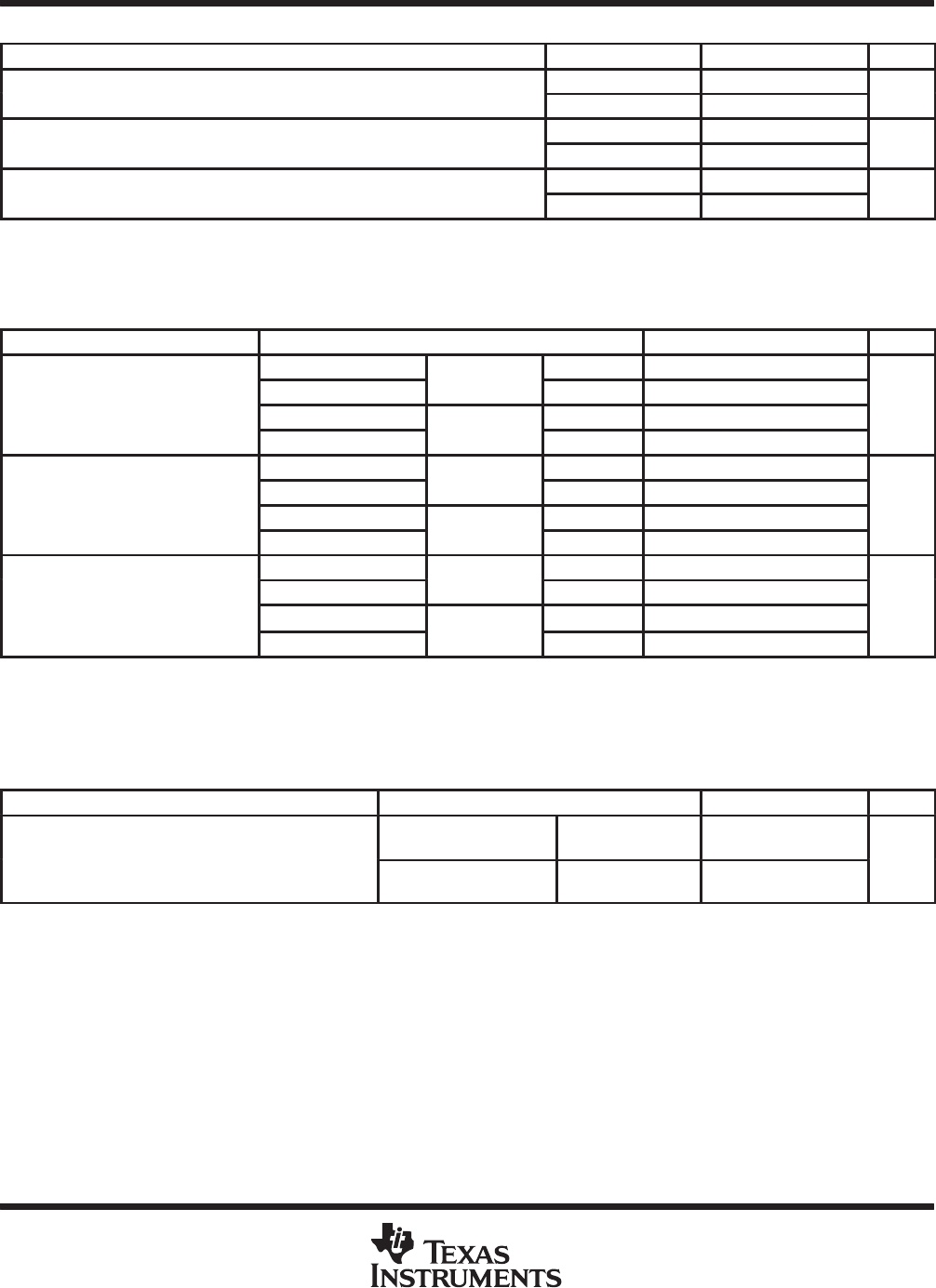
Schmitt-trigger inputs Port P1 to Port P2; P1.0 to P1.7, P2.0 to P2.5
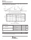
PARAMETER TEST CONDITIONS MIN TYP MAX UNIT
V
IT
Positive going in
p
ut threshold voltage
V
CC
= 2.2 V 1.1 1.3
V
V
IT+
Positi
v
e
-
going
inp
u
t
threshold
v
oltage
V
CC
= 3 V 1.5 1.8
V
V
IT
Negative going in
p
ut threshold voltage
V
CC
= 2.2 V 0.4 0.9
V
V
IT–
Negati
v
e
-
going
inp
u
t
threshold
v
oltage
V
CC
= 3 V .90 1.2
V
V
h
In
p
ut voltage hysteresis (V
IT
V
IT
)
V
CC
= 2.2 V 0.3 1
V
V
hys
Inp
u
t
v
oltage
h
y
steresis
,
(V
IT+
–
V
IT–
)
V
CC
= 3 V 0.5 1.4
V
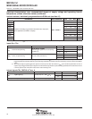
electrical characteristics over recommended ranges of supply voltage and operating free-air
temperature (unless otherwise noted) (continued)
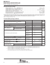
outputs Port 1 to P2; P1.0 to P1.7, P2.0 to P2.5
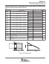
PARAMETER TEST CONDITIONS MIN TYP MAX UNIT
I
(OHmax)
= –1.5 mA
V
CC
=22V
See Note 8 V
CC
–0.25 V
CC
V
OH
High-level output voltage
Port 1 and Port 2 (C11x1)
I
(OHmax)
= –6 mA
V
CC
=
2
.
2
V
See Note 9 V
CC
–0.6 V
CC
V
V
OH
P
or
t
1
an
d
P
or
t
2
(C11
x
1)
Port 1
(
F11x1
)
I
(OHmax)
= –1.5 mA
V
CC
=3V
See Note 8 V
CC
–0.25 V
CC
V
Port
1
(F11x1)
I
(OHmax)
= –6 mA
V
CC
=
3
V
See Note 9 V
CC
–0.6 V
CC
I
(OHmax)
= –1 mA
V
CC
=22V
See Note 10 V
CC
–0.25 V
CC
V
OH
High-level output voltage
I
(OHmax)
= –3.4 mA
V
CC
=
2
.
2
V
See Note 10 V
CC
–0.6 V
CC
V
V
OH
gg
Port 2 (F11x1)
I
(OHmax)
= –1 mA
V
CC
=3V
See Note 10 V
CC
–0.25 V
CC
V
I
(OHmax)
= –3.4 mA
V
CC
=
3
V
See Note 10 V
CC
–0.6 V
CC
I
(OLmax)
= 1.5 mA
V
CC
=22V
See Note 8 V
SS
V
SS
+0.25
V
OL
Low-level output voltage
Port 1 and Port 2 (C11x1
I
(OLmax)
= 6 mA
V
CC
=
2
.
2
V
See Note 9 V
SS
V
SS
+0.6
V
V
OL
P
or
t
1
an
d
P
or
t
2
(C11
x
1
,
F11x1
)
I
(OLmax)
= 1.5 mA
V
CC
=3V
See Note 8 V
SS
V
SS
+0.25
V
F11x1)
I
(OLmax)
= 6 mA
V
CC
=
3
V
See Note 9 V
SS
V
SS
+0.6
NOTES: 8. The maximum total current, I
OHmax
and I
OLmax
, for all outputs combined, should not exceed ±12 mA to hold the maximum voltage
drop specified.
9. The maximum total current, I
OHmax
and I
OLmax
, for all outputs combined, should not exceed ±48 mA to hold the maximum voltage
drop specified.
10. One output loaded at a time.
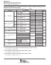
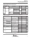
leakage current
PARAMETER TEST CONDITIONS MIN TYP MAX UNIT
I
lk (P )
High im
p
edance leakage current
Port P1: P1.x, 0 ≤ ×≤ 7
(see Notes 11, 12)
V
CC
= 2.2 V/3 V,
±50
nA
I
lkg(Px.x)
High
-
impedance
leakage
c
u
rrent
Port P2: P2.x, 0 ≤ ×≤ 5
(see Notes 11, 12)
V
CC
= 2.2 V/3 V,
±50
nA
NOTES: 11. The leakage current is measured with V
SS
or V
CC
applied to the corresponding pin(s), unless otherwise noted.
12. The leakage of the digital port pins is measured individually. The port pin must be selected for input and there must be no optional
pullup or pulldown resistor.