


MSP430x11x1
MIXED SIGNAL MICROCONTROLLER
SLAS241C – SEPTEMBER 1999 – REVISED JUNE 2000
20
POST OFFICE BOX 655303 • DALLAS, TEXAS 75265
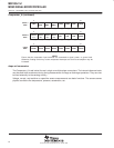
digital I/O (continued)
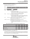
The seven registers are:
• Input register 8 bits at port P1/P2 contains information at the pins
• Output register 8 bits at port P1/P2 contains output information
• Direction register 8 bits at port P1/P2 controls direction
• Interrupt edge select 8 bits at port P1/P2 input signal change necessary for interrupt
• Interrupt flags 8 bits at port P1/P2 indicates if interrupt(s) are pending
• Interrupt enable 8 bits at port P1/P2 contains interrupt enable bits
• Selection (Port or Mod.) 8 bits at port P1/P2 determines if pin(s) have port or module function
All these registers contain eight bits. Two interrupt vectors are implemented: one commonly used for any
interrupt event on ports P1.0 to P1.7, and one commonly used for any interrupt event on ports P2.0 to P2.7.
NOTE:
Six bits of port P2, P2.0 to P2.5, are available on external pins – but all control and data bits for port
P2 are implemented.
watchdog timer
The primary function of the watchdog timer (WDT) module is to perform a controlled system restart after a
software problem has occurred. If the selected time interval expires, a system reset is generated. If this
watchdog function is not needed in an application, the module can work as an interval timer, which generates
an interrupt after the selected time interval.
The watchdog timer counter (WDTCNT) is a 16-bit up-counter which is not directly accessible by software. The
WDTCNT is controlled through the watchdog timer control register (WDTCTL), which is a 16-bit read/write
register. Writing to WDTCTL is, in both operating modes (watchdog or timer), only possible by using the correct
password in the high-byte. The low-byte stores data written to the WDTCTL. The high-byte must be the
password 05Ah. If any value other than 05Ah is written to the high-byte of the WDTCTL, a system reset PUC
is generated. When the password is read, its value is 069h. This minimizes accidental write operations to the
WDTCTL register. In addition to the watchdog timer control bits, there are two bits included in the WDTCTL
register that configure the NMI pin.
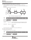
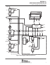
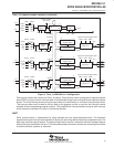
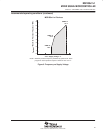
Timer_A (Three capture/compare registers)
The Timer_A module on 11x1 devices offers one sixteen bit counter and three capture/compare registers. The
timer clock source can be selected to come from two external sources TACLK (SSEL=0) or INCLK (SSEL=3),
or from two internal sources, the ACLK (SSEL=1) or SMCLK (SSEL=2). The clock source can be divided by
one, two, four, or eight. The timer can be fully controlled (in word mode) since it can be halted, read, and written.
It can be stopped, run continuously, counted up or up/down, using one compare block to determine the period.
The three capture/compare blocks are configured by the application to run in capture or compare mode.
The capture mode is primarily used to measure external or internal events using any combination of positive,
negative, or both edges of the signal. Capture mode can be started and stopped by software. Three different
external events TA0, TA1, and TA2 can be selected. At capture/compare register CCR2 the ACLK is the capture
signal if CCI2B is selected. Software capture is chosen if CCISx=2 or CCISx=3 (see Figure 4).
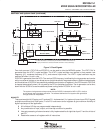
The compare mode is primarily used to generate timings for the software or application hardware, or to generate
pulse-width modulated output signals for various purposes like D/A conversion functions or motor control. An
individual output module is assigned to each of the three capture/compare registers. The output modules can
run independently of the compare function, or can be triggered in several ways.