


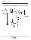
MSP430x11x1
MIXED SIGNAL MICROCONTROLLER
SLAS241C – SEPTEMBER 1999 – REVISED JUNE 2000
30
POST OFFICE BOX 655303 • DALLAS, TEXAS 75265
electrical characteristics over recommended ranges of supply voltage and operating free-air
temperature (unless otherwise noted) (continued)
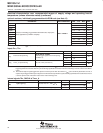
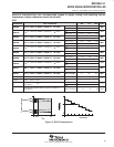
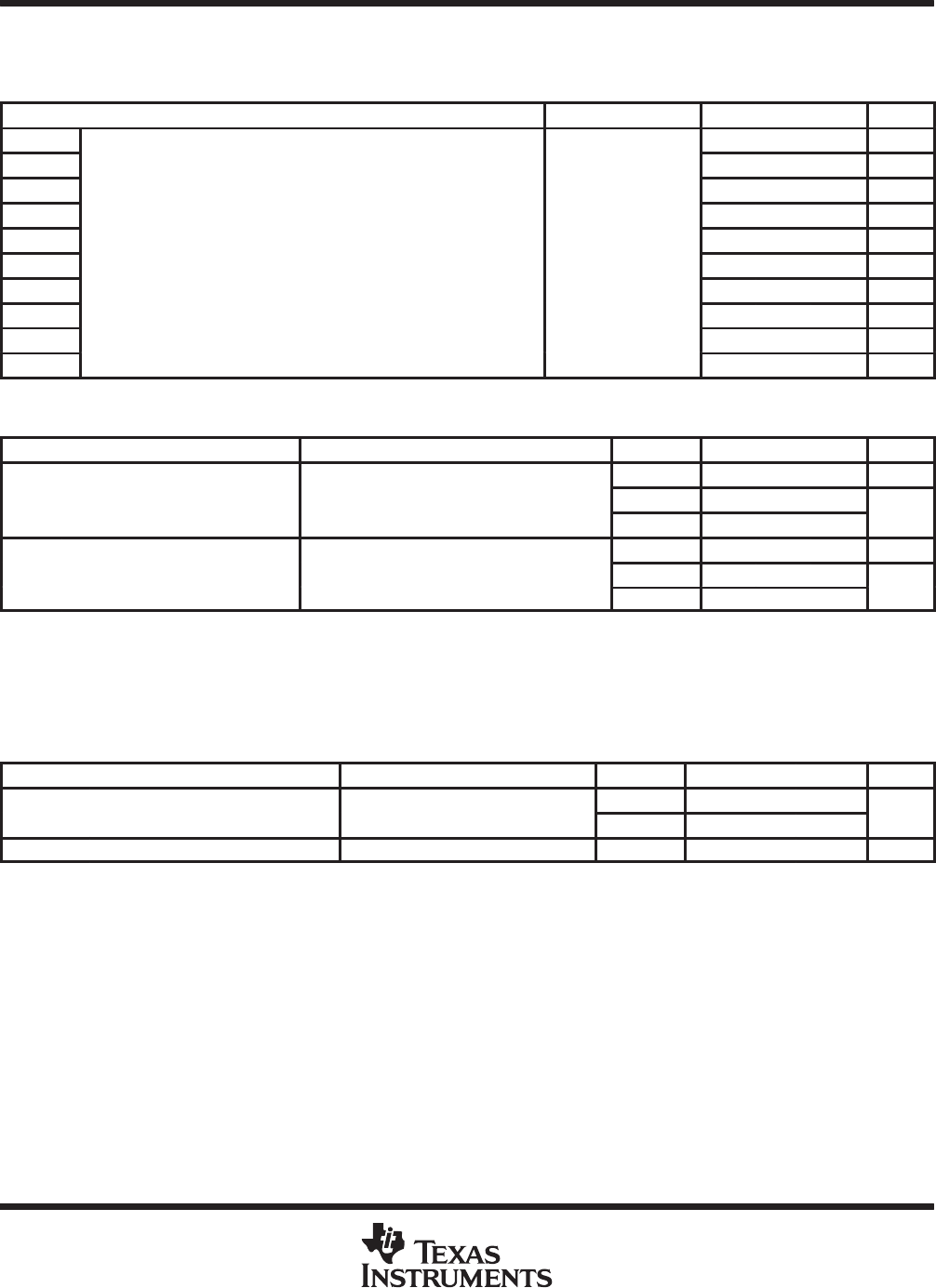
optional resistors, individually programmable with ROM code (see Note 13)
PARAMETER TEST CONDITIONS MIN TYP MAX UNIT
R
(opt1)
2.5 5 10 kΩ
R
(opt2)
3.8 7.7 15 kΩ
R
(opt3)
7.6 15 31 kΩ
R
(opt4)
11.5 23 46 kΩ
R
(opt5)
Resistors, individually programmable with ROM code, all port pins,
V
CC
= 2 2 V/3 V
23 45 90 kΩ
R
(opt6)
yg
values applicable for pulldown and pullup
V
CC
=
2
.
2
V/3
V
46 90 180 kΩ
R
(opt7)
70 140 280 kΩ
R
(opt8)
115 230 460 kΩ
R
(opt9)
160 320 640 kΩ
R
(opt10)
205 420 830 kΩ
NOTE 13: Optional resistors R
optx
for pulldown or pullup are not available in standard flash memory device MSP430F11x1.
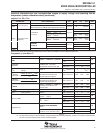
inputs Px.x, TAx
PARAMETER TEST CONDITIONS VCC MIN TYP MAX UNIT
Port P1, P2: P1.x to P2.x,
2.2 V/3 V 1.5 cycle
t
(int)
External interrupt timing
Port
P1
,
P2:
P1
.
x
to
P2
.
x
,
External trigger signal for the interrupt flag,
2.2 V 62
ns
()
(see Note 14)
3 V 50
ns
2.2 V/3 V 1.5 cycle
t
(cap)
Timer_A, capture timing TA0, TA1, TA2. (see Note 15)
2.2 V 62
ns
()
3 V 50
ns
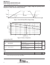
NOTES: 14. The external signal sets the interrupt flag every time the minimum t
int
cycle and time parameters are met. It may be set even with
trigger signals shorter than t
int
. Both the cycle and timing specifications must be met to ensure the flag is set. t
int
is measured in MCLK
cycles.
15. The external capture signal triggers the capture event every time when the minimum t
cap
cycles and time parameters are met. A
capture may be triggered with capture signals even shorter than t
cap
. Both the cycle and timing specifications must be met to ensure
a correct capture of the 16-bit timer value and to ensure the flag is set.
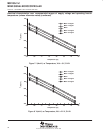
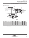
internal signals TAx, SMCLK at Timer_A
PARAMETER TEST CONDITIONS VCC MIN TYP MAX UNIT
f
(IN)
In
p
ut frequency
Internal TA0 TA1 TA2 t
H
=t
L
2.2 V 8
MHz
f
(IN)
Inp
u
t
freq
u
enc
y
Internal
TA0
,
TA1
,
TA2
,
t
H
=
t
L
3 V 10
MH
z
f
(TAint)
Timer_A clock frequency Internally, SMCLK signal applied 2.2 V/3 V dc f
System