


MSP430x11x1
MIXED SIGNAL MICROCONTROLLER
SLAS241C – SEPTEMBER 1999 – REVISED JUNE 2000
41
POST OFFICE BOX 655303 • DALLAS, TEXAS 75265
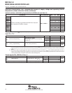
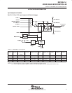
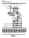
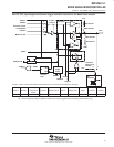
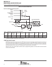
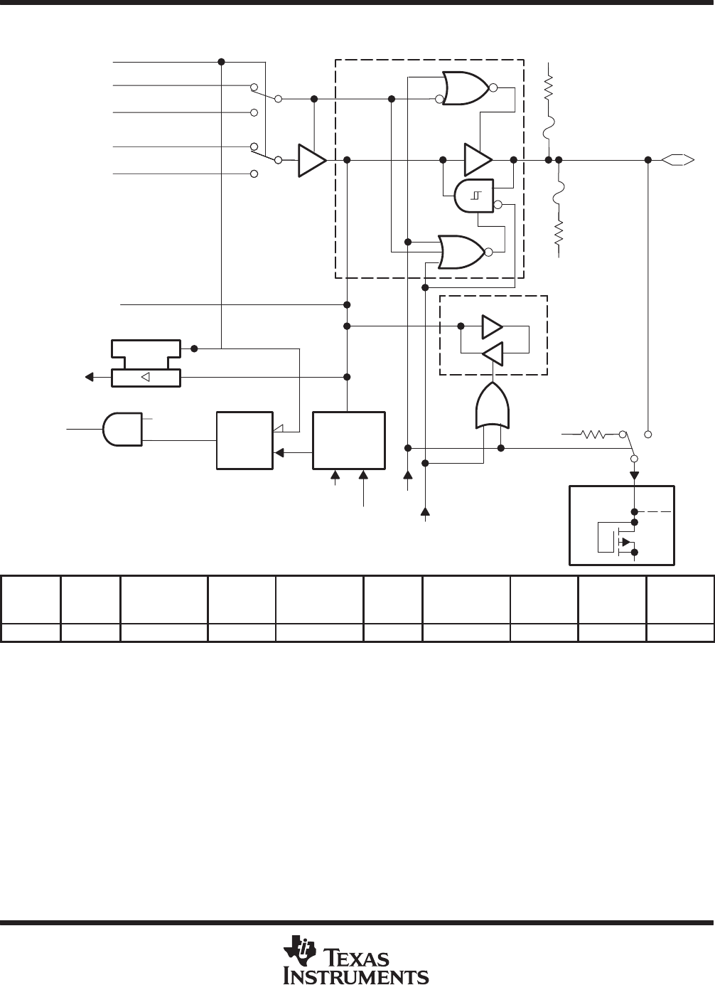
Port P2, P2.5, input/output with Schmitt-trigger and R
OSC
function for the Basic Clock module
EN
D
See Note 27
See Note 28
See Note 28
See Note 27
GND
V
CC
P2.5
0
1
0
1
Interrupt
Edge
Select
EN
Set
Q
P2IE.5
P2IFG.5
P2IRQ.5
Interrupt
Flag
P2IES.5
P2SEL.5
Module X IN
P2IN.5
P2OUT.5
Module X OUT
Direction Control
From Module
P2DIR.5
P2SEL.5
Pad Logic
NOTE: DCOR: Control bit from Basic Clock Module if it is set, P2.5 Is disconnected from P2.5 pad
Bus Keeper
0
1
0
1
V
CC
Internal to
Basic Clock
Module
DCOR
DC
Generator
0: Input
1: Output
CAPD.5
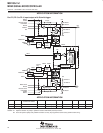
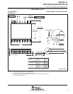
PnSel.x PnDIR.x
Direction
control from
module
PnOUT.x Module X OUT PnIN.x Module X IN PnIE.x PnIFG.x PnIES.x
P2Sel.5 P2DIR.5 P2DIR.5 P2OUT.5 VSS P2IN.5 unused P2IE.5 P2IFG.5 P2IES.5
NOTES: 27. Optional selection of pullup or pulldown resistors with ROM (masked) versions.
28. Fuses for optional pullup and pulldown resistors can only be programmed at the factory (ROM versions only).