


MSP430x11x1
MIXED SIGNAL MICROCONTROLLER
SLAS241C – SEPTEMBER 1999 – REVISED JUNE 2000
3
POST OFFICE BOX 655303 • DALLAS, TEXAS 75265
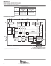
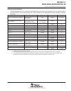
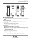
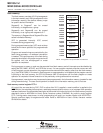
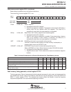
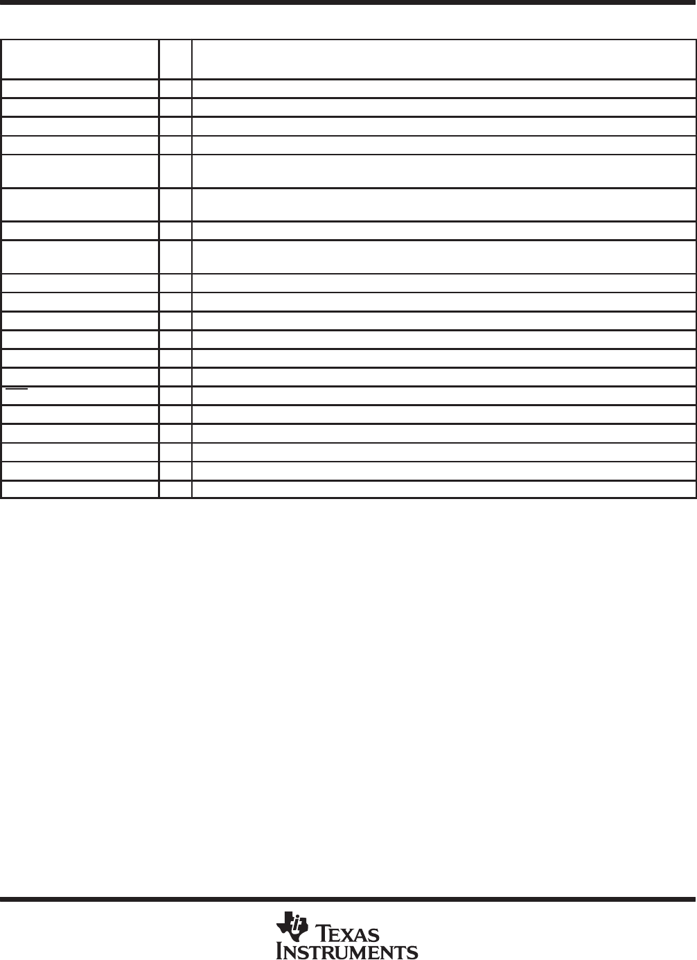
Terminal Functions
TERMINAL
TERMINAL
I/O
DESCRIPTION
NAME NO.
I/O
DESCRIPTION
P1.0/TACLK 13 I/O General-purpose digital I/O pin/Timer_A, clock signal TACLK input
P1.1/TA0 14 I/O General-purpose digital I/O pin/Timer_A, capture: CCI0A input, compare: Out0 output
P1.2/TA1 15 I/O General-purpose digital I/O pin/Timer_A, capture: CCI1A input, compare: Out1 output
P1.3/TA2 16 I/O General-purpose digital I/O pin/Timer_A, capture: CCI2A input, compare: Out2 output
P1.4/SMCLK/TCK 17 I/O General-purpose digital I/O pin/SMCLK signal output/test clock, input terminal for device programming
and test
P1.5/TA0/TMS 18 I/O General-purpose digital I/O pin/Timer_A, compare: Out0 output/test mode select, input terminal for
device programming and test
P1.6/TA1/TDI 19 I/O General-purpose digital I/O pin/Timer_A, compare: Out1 output/test data input terminal
P1.7/TA2/TDO/TDI
†
20 I/O General-purpose digital I/O pin/Timer_A, compare: Out2 output/test data output terminal or data input
during programming
P2.0/ACLK 8 I/O General-purpose digital I/O pin/ACLK output
P2.1/INCLK 9 I/O General-purpose digital I/O pin/Timer_A, clock signal at INCLK
P2.2/CAOUT/TA0 10 I/O General-purpose digital I/O pin/Timer_A, capture: CCI0B input/comparator_A, output
P2.3/CA0/TA1 11 I/O General-purpose digital I/O pin/Timer_A, compare: Out1 output/comparator_A, input
P2.4/CA1/TA2 12 I/O General-purpose digital I/O pin/Timer_A, compare: Out2 output/comparator_A, input
P2.5/R
osc
3 I/O General-purpose digital I/O pin/Input for external resistor that defines the DCO nominal frequency
RST/NMI 7 I Reset or nonmaskable interrupt input
TEST 1 I Select of test mode for JTAG pins on Port1. Must be tied low with less than 30 kΩ (F11x1).
VCC 2 Supply voltage
V
SS
4 Ground reference
XIN 6 I Input terminal of crystal oscillator
XOUT 5 I/O Output terminal of crystal oscillator
†
TDO or TDI is selected via JTAG instruction.
short-form description
processing unit
The processing unit is based on a consistent, and orthogonally-designed CPU and instruction set. This design
structure results in a RISC-like architecture, highly transparent to the application development, and noted for
its programming simplicity. All operations other than program-flow instructions are consequently performed as
register operations in conjunction with seven addressing modes for source, and four modes for destination
operands.