TPS56xx Functions
2-2
2.1 TPS56xx Functions
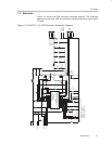
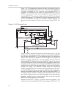
The functional block diagram of the TPS56xx family of controllers is given in
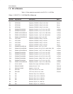
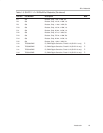
Figure 2–1. The controller has the following main features:
- ±1% reference over 0°C to125°C junction temperature range.
- Synchronous-buck gate drivers with adaptive deadtime control
- High-side MOSFET driver voltage rating of 30 V
- MOSFET driver peak current rating of 2 A
- Hysteretic comparator: 250-ns propagation delay to gate driver outputs,
2.5-mV offset voltage, symmetrical hysteresis, hysteresis setting is a
percentage of Vref.
- Lossless output current sensing circuit
- Slowstart circuit; slowstart time independent of VID setting
- Internal 8-V drive regulator for reduced gate charge power losses
- POWERGOOD comparator, 93% of Vref trip
- UVLO, Vcc undervoltage lockout, 10-V start, 2-V hysteresis
- INHIBIT comparator that can also monitor UVLO of the system logic
supply, 2.1-V start, 100-mV hysteresis.
- Latched overcurrent shutdown circuit
- Latched overvoltage shutdown circuit
- LODRV pin that activates the low-side MOSFETs as a crowbar to protect
against a short across the high-side MOSFETs.


