TPS56xx Functions
2-13
Design Procedure
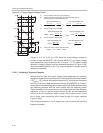
LOHIB (pin 11) is an inhibit input for the low-side MOSFET driver. This input
has to be logic low before the low-side MOSFET is allowed to be turned on,
i.e., a logic high on LOHIB prevents the low-side MOSFET driver from turning
on the low-side MOSFET. For normal synchronous operation, this pin is
connected to the junction of the high and low-side MOSFETs. This prevents
cross-conduction of the two MOSFETs by constraining the low-side MOSFET
to be OFF unless its drain-to-source voltage is at a low level. Shoot-through
current caused by both MOSFETs being ON simultaneously is actively
prevented. However, if LODRV is low, the low-side MOSFET is turned ON
regardless of the LOHIB input.
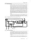
2.1.10.2 High-Side Driver
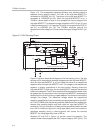
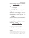
The driver for the high-side MOSFET can be configured either as a
ground-referenced driver or as a floating bootstrap driver. When configured as
a floating driver, the bias voltage to the driver is developed from the DRV
regulator. The maximum voltage that can be applied between BOOT and
DRVGND is 30 V. The driver can be referenced to ground by connecting
BOOTLO to DRVGND, and connecting VCC to BOOT. A 1-µF capacitor, C7, is
connected from BOOT (pin 16) to BOOTLO (pin 18) for bypassing.
2.1.10.3 Grounding
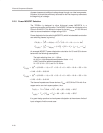
Three separate ground connections enable the user to isolate high-current
grounds from low current logic grounds. The low-current logic ground is called
analog
ground
.
ANAGND (pin 7) and AGND2 (pin2) are the connections for
analog ground
.
The high-current ground is called power
ground and must be
connected to DRVGND (pin 12). The maximum voltage difference between
ANAGND and DRVGND must be limited to less than ±0.2 V.
Refer to the
Layout Guidelines
section of the TPS56xx data sheet for further
information on grounding.


