


TPS56xx Functions
2-12
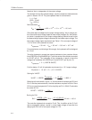
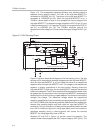
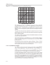
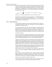
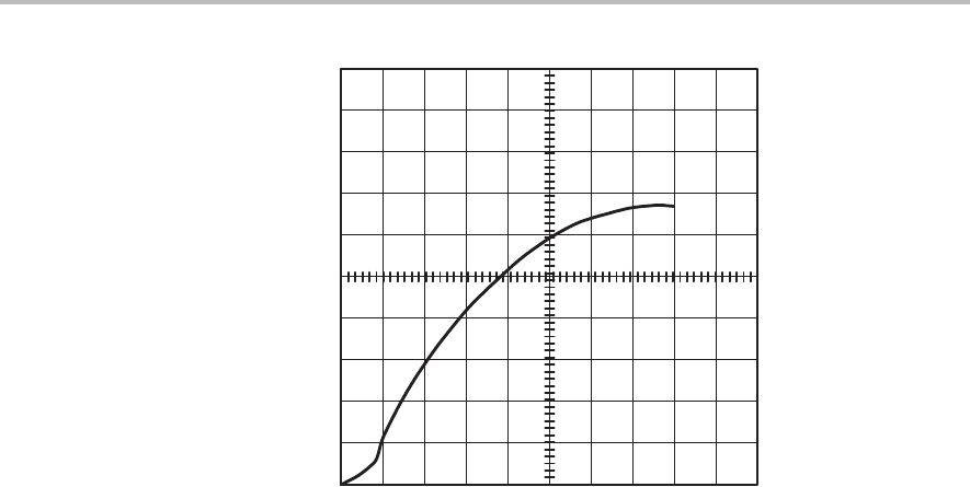
Figure 2–5. I–V Characteristic Curve for Low-Side Gate Drivers
Driver Output Voltage – 1 V/div
Driver Sink Current – 0.5 A/div
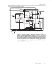
The high-side gate driver is a bootstrap configuration with an internally
integrated Schottky bootstrap diode. The voltage rating of the BOOT pin to
DRVGND is 30 V. The gate drivers are biased from an internal 8-V drive
regulator to minimize the gate drive power losses that are dissipated inside the
TPS55xx.
The gate drivers have also been optimized to reduce the amount of internal
shoot-through current, which will result when either the low-side or high-side
driver is switching states.
The adaptive deadtime control minimizes the deadtime between conduction
intervals of the power MOSFETs.
The low-side gate driver is not allowed to turn on until the Vphase voltage is
below 2 V; the high-side gate driver is not allowed to turn on until the LOWDR
pin falls below 2 V.
Fast switching and short dead times improve efficiency. There is 100-mA
current limiting within the internal 8-V voltage regulator to protect the regulator
and IC against a short fault on one of the driver pins.
2.1.10.1 Low-Side Driver Controls
The TPS56xx contains two control inputs to control the low-side MOSFET
drive for various applications. They are LODRV (pin 10) and LOHIB (pin 11).
LODRV (pin 10) is an enable input for the low-side MOSFET driver. This pin
is connected to the 5-V input supply for normal synchronous operation.
For added overvoltage protection, external sensing circuitry can be included
to drive the LODRV input low in the event of an overvoltage. Applying a logic
low to LODRV causes the driver for the low-side MOSFET to go to a high state
causing the low-side MOSFET to turn on and act as a crowbar for the output.
This input has precedence over any input present at LOHIB (pin 11); i.e., a low
input to LODRV (pin 10) overrides the inhibit function.