External Component Selection
2-20
of power losses and additional voltage drops through non-ideal components.
Equation (4) should be sufficiently accurate for the first frequency estimate at
the beginning of a design.
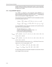
2.2.5 Power MOSFET Selection
The TPS56xx is designed to drive N-channel power MOSFETs in a
synchronous rectifier configuration. The MOSFET chosen for this design is the
Siliconix Si4410DY. This device is chosen for its low r
DS(on)
of 13.5 mΩ and
drain-to-source breakdown voltage rating of 30 V.
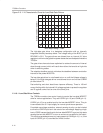
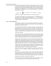
Power dissipation for the switching MOSFETs, which includes both conduction
and switching losses, is given by:
P
D
(
Q
1)
+
ǒ
I
2
O
r
DS
(
on
)
D
Ǔ
)
ǒ
0.5
V
i
I
O
t
r
)
f
f
sw
Ǔ
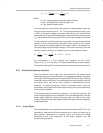
P
D
(
Q
2)
+
ǒ
I
2
O
r
DS
(
on
)
(
1
–D
)
Ǔ
)
ǒ
0.5
V
i
I
O
t
r
)
f
f
sw
Ǔ
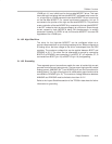
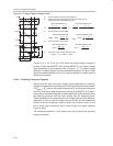
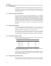
An example MOSFET power dissipation calculation for Q1 and Q3 is shown
below with the following assumptions:
The total switching time,
t
r+f
= 100 ns,
An
r
DS
(on)
high temperature adjustment factor = 1.4,
A 60°C maximum ambient temperature,
V
I
= 5.0 V, V
O
= 3.3 V, and I
O
= 6 A then :
P
D
(
Q
1)
+
(
6
)
2
(
0.0135 1.4
)
0.7 ) 0.5 5 6 100 10
–
9
135 10
3
+ 0.48 ) 0.20 + 0.68
W
P
D
(
Q
2)
+
(
6
)
2
(
0.0135 1.4
)
0.3 ) 0.5 5 6 100 10
–
9
135 10
3
+ 0.20 ) 0.20 + 0.40
W
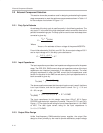
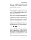
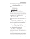
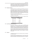
The thermal impedance of these devices, R
θJA
= 90°C/W for FR-4 with 2-oz.
copper and a one-inch-square pattern, thus:
T
J
(
Q
1)
+
T
A
)
ǒ
R
q
JA
P
D
Ǔ
+ 60 )
(
50 0.90
)
+ 94°
C
T
J
(
Q
2)
+
T
A
)
ǒ
R
q
JA
P
D
Ǔ
+ 60 )
(
50 1.40
)
+ 80°
C
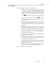
It is good design practice to check power dissipation at the extreme limits of
input voltage to find the worst case.


