


TPS56xx Functions
2-3
Design Procedure
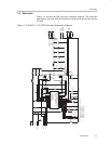
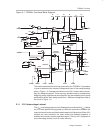
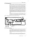
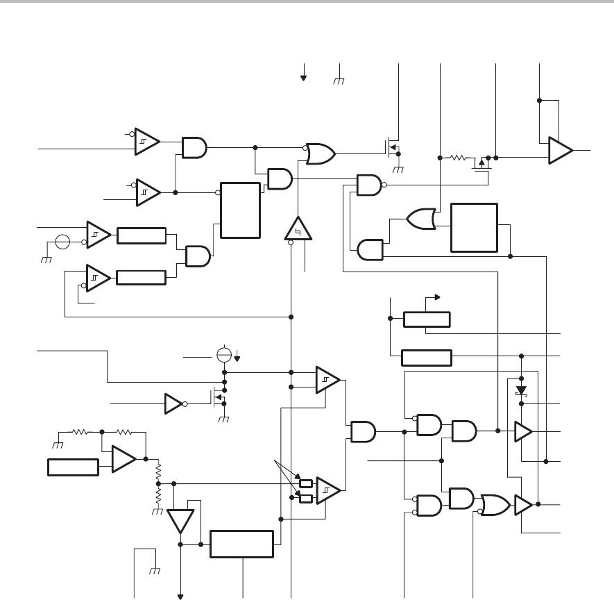
Figure 2–1. TPS56xx Functional Block Diagram
INHIBIT
OCP
SLOWST
IOUT
BIAS
DRV
BOOT
HIGHDR
BOOTLO
LOWDR
DRVGND
HISENSEIOUTLOLOSENSEPWRGDANAGND
CC
V
VREFBAGND2 VSENSEVHYST LODRVLOHIB
_
+
2 V
10 V
UVLO
V
CC
22
3
8
25 4 6 11 10
15 7 28 20
21
19
1
9
14
16
17
18
13
12
_
+
Deglitch
100mV
VOVP
1.15 VREF
VSENSE
S
R
Q
V
CC
Deglitch
Fault
Shutdown
VPGD
0.93 VREF
Rising
Edge
Delay
HIGHIN
HIGHDR
2X
Shutdown
_
+
Bandgap
_
+
I
VREFB
5
Analog
Bias
VREF
Hysteresis
Setting
I
VREFB
_
+
_
+
Hysteresis
Comparator
Shutdown
Slowstart
Comparator
CM Filters
PREREG
DRV REG
V
CC
Analog
Bias
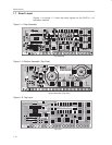
This section describes the functions governed by the TPS556xx. A procedure
is given to determine the values of components used in the example design
given in Figure 1–3. Example calculations for the 3.3-V output version accom-
pany the design equations. There are many possible ways to proceed when
designing power supplies and some iteration may be necessary when actual
performance differs from design predictions. Reference designators refer to
the circuit in Figure 1–3.
2.1.1 V
CC
Undervoltage Lockout
The V
CC
undervoltage lockout circuit disables the controller while V
CC
is below
the 10-V start threshold during power up. While the controller is disabled, the
output drivers will be low and the slowstart capacitor will be shorted. When V
CC
exceeds the start threshold, the short across the slowstart capacitor is
released and normal converter operation begins. There is a 2-V hysteresis in
the undervoltage lockout circuit for noise immunity.