TPS56xx Functions
2-5
Design Procedure
R
VREFB
+
3.3
V
165 m
A
+ 20
k
W
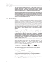
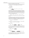
This value is used to determine the values of R10 and R14 that set the
hysteresis level.
The equations above can be used to derive a simplified relationship for the
slowstart time as shown:
t
SLOWSTART
+ 5
C
SLOWSTART
R
VREFB
V
O
start-up waveforms for different reference voltage settings are given in
Figures 3–7, 3–8, 3–9, 3–16, 3–17, 3–18, 3–25, 3–26, 3–27, 3–34, 3–35, and
3–36 in the test results section, showing that slowstart time is independent of
the reference voltage.
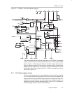
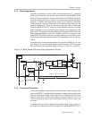
2.1.4 Hysteresis Setting
The next step in this design is choosing the desired output voltage ripple. As
a first approximation, the output voltage ripple is simply the difference between
the two levels (V
LO
and V
Hi
) shown in Figure 1–2. The hysteresis setting of
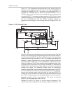
the hysteresis comparator of the TPS56xx sets these two levels. The
hysteresis is set by two external resistors and is centered around VREF (pin
5). The hysteretic comparator is designed with low input offset voltage
(±2.5 mV max) low propagation delays (250ns max to gate driver outputs with
10mV overdrive) and accurate hysteresis setting (±3.5 mV max). The
hysteresis is proportional to the reference voltage; setting Vref to a new value
automatically adjusts the hysteresis to be the same percentage of Vref.
The total output ripple is greater than the ripple set by the hysteresis compara-
tor. To accurately choose the output voltage ripple, all of the propagation de-
lays must be considered. The first step is to calculate the amount of ripple ex-
pected due to the delays, in addition to the ripple set by the hysteresis compa-
rator. Using the terminology of Section 2.2.4.1, this additional ripple is equal
to V
p-p
– Hyst and will be referred to V
del
for ease of reference. Or:
V
p-p
+
Hyst
)
V
del
Where:
V
p-p
=the total output ripple,
Hyst = the hysteresis setting of the hysteretic comparator, and
V
del
= the output ripple exceeding Hyst and due to all propagation
delays.
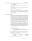
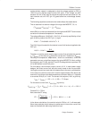
Assuming the output ripple during the delay time is primarily caused by the
inductor ripple current flowing through the output capacitors’ ESR, the
additional ripple, V
del
, can be estimated as:
V
del
+
ƪ
V
I
–V
O
L
t
del
ƫ
ESR
)
ƪ
V
O
L
t
del
ƫ
ESR
+
V
I
t
del
L
Where L is the value of the output inductor.


