TPS56xx Functions
2-4
2.1.2 Inhibit
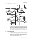
The inhibit circuit is a comparator with a 2.1-V start voltage and a 100-mV
hysteresis. When inhibit is low, the output drivers are low and the slowstart
capacitor is discharged. When inhibit is above the start threshold, the short
across the slowstart capacitor is released and normal operation begins.
When the system logic supply is connected to the inhibit pin, the inhibit pin also
controls power sequencing by locking out controller operation until the system
logic supply exceeds the input threshold voltage of the inhibit circuit; thus, the
12-V supply and the system logic supply must be above UVLO thresholds
before the controller is allowed to start up.
2.1.3 Slowstart Design
Slowstart or soft-start is added to reduce power-up transients. Without
slowstart, when input power is first applied, the TPS56xx attempts to raise the
output voltage (initially zero) to its normal operating level by turning on the top
MOSFET until the voltage is approximately Vref. This can cause high transient
currents to flow in the output inductor and output capacitor. Although this form
of startup usually does not cause component failures, it does apply stresses
much greater than those typically encountered in normal operation. It is good
design practice to include slowstart circuitry to avoid these unnecessary
stresses.
The slowstart circuit in the TPS56xx controls the rate at which the output
voltage powers up. A capacitor, C21, connected between SLOWST (pin 8) and
ANAGND (pin 7), is charged by an internal current source. This current source
is proportional to the reference voltage and is adjustable by an external
resistance selected by the user. The output voltage follows the voltage on the
slowstart capacitor during startup. Since the charging current is proportional
to the reference voltage, the slowstart time is independent of the reference
voltage for a given resistor value.
Choices of the slowstart time and the slowstart capacitor value are largely
arbitrary as long as system start-up time requirements are met. For this
example design, a slowstart time of 10 ms is chosen, and the slowstart
capacitor is chosen to be 0.1 µF. Therefore, to charge 0.1 µF from zero volts
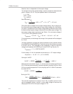
to 3.3 V in 10 ms, the following equation holds:
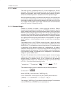
I
SLOWSTART
+
C
SLOWSTART
D
V
c
D
t
ss
+ 0.1 m
F
3.3
V
10
ms
+ 33 m
A
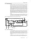
The slowstart charging current is determined by the following equation:
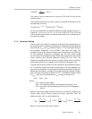
I
SLOWSTART
+
I
(
VREFB
)
5
where I(VREFB) = the current out of VREFB (pin 5).
For an I
SLOWSTART
current equal to 33 µA, I(VREFB) should be set to:
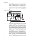
I
(
VREFB
)
+ 5
I
SLOWSTART
+ 5 33 m
A
+ 165 m
A
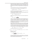
The voltage on VREFB (pin 5) is a buffered reference voltage. The resistance
from the VREFB pin to ANAGND can be calculated as:


