


Ethernet 1000BASE-X PCS/PMA or SGMII v9.1 www.xilinx.com 169
UG155 March 24, 2008
Required Constraints
R
Clock Period Constraints
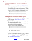
The clocks provided to pma_rx_clk0 and pma_rx_clk1 must be constrained for a clock
frequency of 62.5 MHz. The clock provided to gtx_clk must be constrained for a clock
frequency of 125 MHz. The following UCF syntax shows the constraints being applied to
the example design.
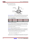
############################################################
# TBI Clock period Constraints: please do not relax #
############################################################
NET "pma_rx_clk0" TNM_NET = "pma_rx_clk0";
TIMESPEC "ts_pma_rx_clk0" = PERIOD "pma_rx_clk0" 16000 ps HIGH 50 %;
NET "pma_rx_clk1" TNM_NET = "pma_rx_clk1";
TIMESPEC "ts_pma_rx_clk1" = PERIOD "pma_rx_clk1" 16000 ps HIGH 50 %;
NET "gtx_clk_bufg" TNM_NET = "clk_tx";
TIMESPEC "ts_tx_clk" = PERIOD "clk_tx" 8000 ps HIGH 50 %;
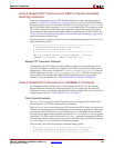
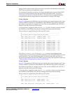
Period constraints should be applied to cover signals in to and out of the block memory
based 8B/10B encoder and decoder.
# Constrain between flip-flops and the Block Memory for the 8B10B
encoder and decoder
INST "gig_eth_pcs_pma_core/BU2/U0/PCS_OUTPUT/DECODER/LOOK_UP_TABLE"
TNM = "codec8b10b";
INST "gig_eth_pcs_pma_core/BU2/U0/PCS_OUTPUT/ENCODER/LOOK_UP_TABLE"
TNM = "codec8b10b";
TIMESPEC "ts_ffs_to_codec8b10b" = FROM FFS TO "codec8b10b" 8000 ps;
TIMESPEC "ts_codec8b10b_to_ffs" = FROM "codec8b10b" TO FFS 8000 ps;
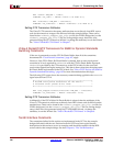
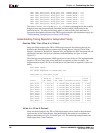
Ten-Bit Interface IOB Constraints
The following constraints target the flip-flops that are inferred in the top level HDL file for
the example design. Constraints are set to ensure that these are placed in IOBs.
INST "tx_code_group_reg*" IOB = true;
INST "ewrap_reg" IOB = true;
INST "en_cdet_reg" IOB = true;
INST "rx_code_group0_reg*" IOB = true;
INST "rx_code_group1_reg*" IOB = true;
Note: For Virtex-4 and Virtex-5 devices, the example design will directly instantiate IOB DDR
components and the previous constraints are not included.
The Ten-Bit Interface (TBI) is a 3.3 volt signal level interface. The 3.3 volt LVTTL SelectIO
standard is the default for Virtex-II devices. The following constraints may safely be
added. The 3.3 volt LVTTL SelectIO standard is not the default for other families. Use the
following constraints and take into account the device IO Banking rules when fixing PADs.
INST "tx_code_group<?>" IOSTANDARD = LVTTL;
INST "pma_tx_clk" IOSTANDARD = LVTTL;
INST "rx_code_group<?>" IOSTANDARD = LVTTL;
INST "pma_rx_clk0" IOSTANDARD = LVTTL;
INST "loc_ref" IOSTANDARD = LVTTL;
INST "ewrap" IOSTANDARD = LVTTL;
INST "en_cdet" IOSTANDARD = LVTTL;