


Ethernet 1000BASE-X PCS/PMA or SGMII v9.1 www.xilinx.com 75
UG155 March 24, 2008
Ten-Bit-Interface Logic
R
Virtex-5 Devices
Method 1
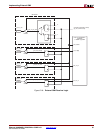
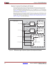
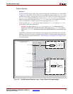
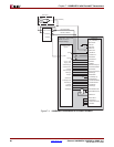
The Virtex-5 FPGA logic used by the example design delivered with the core is illustrated
in Figure 6-6. This shows a Virtex-5 device IDDR primitive used with the DDR_CLK_EDGE
attribute set to SAME_EDGE (see the Virtex-5 FPGA User Guide). This uses local inversion of
pma_rx_clk0 within the IOB logic to receive the rx_code_group[9:0] data bus on
both the rising and falling edges of pma_rx_clk0. The SAME_EDGE attribute causes the
IDDR to output both Q1 and Q2 data on the rising edge of pma_rx_clk0.
For this reason, pma_rx_clk0 can be routed to both pma_rx_clk0 and pma_rx_clk1
clock inputs of the core as illustrated.
Caution!
This logic relies on pma_rx_clk0 and pma_rx_clk1 being exactly 180
degrees out of phase with each other because the falling edge of pma_rx_clk0 is used in
place of pma_rx_clk1. See the data sheet for the attached SERDES to verify that this is the
case.
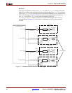
The IODELAY elements can be adjusted to fine-tune the setup and hold times at the TBI
IOB input flip-flops. The delay is applied to the IODELAY element using constraints in the
UCF; these can be edited if desired. See “Ten-Bit Interface Constraints” in Chapter 12 for
more information.
Figure 6-6: Ten-Bit Interface Receiver Logic - Virtex-5 Device (Example Design)
component_name
_block (Block Level from example design)
pma_rx_clk0
IBUFG
IOB LOGIC
IPAD
rx_code_group[0]
IBUF
IPAD
Ethernet 1000BASE-X PCS/PMA
or SGMII LogiCORE
pma_rx_clk0
BUFG
IOB LOGIC
pma_rx_clk1
rx_code_group0[0]
rx_code_group1[0]
rx_code_group1_reg[0]
rx_code_group0_reg[0]
IDDR
Q1
D
Q2
C
IODELAY
IODELAY