


Ethernet 1000BASE-X PCS/PMA or SGMII v9.1 www.xilinx.com 203
UG155 March 24, 2008
Post-Implementation Simulation
R
layout and timing requirements specified within the PCF file. The par command outputs
the placed and routed physical design to an NCD file.
An example of the par command is:
$ par top_level_module_name_map.ncd top_level_module_name.ncd \
top_level_module_name.pcf
Static Timing Analysis
The trce command must be executed to evaluate timing closure on a design and create a
Timing Report file (TWR) that is derived from static timing analysis of the Physical Design
file (NCD). The analysis is typically based on constraints included in the optional PCF file.
An example of the trce command is:
$ trce -o top_level_module_name.twr top_level_module_name.ncd \
top_level_module_name.pcf
Generating a Bitstream
The bitgen command must be executed to create the configuration bitstream (BIT) file
based on the contents of a physical implementation file (NCD). The BIT file defines the
behavior of the programmed FPGA.
An example of the bitgen command is:
$ bitgen -w top_level_module_name.ncd
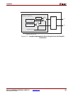
Post-Implementation Simulation
The purpose of post-implementation simulation is to verify that the design as
implemented in the FPGA works as expected.
Generating a Simulation Model
To generate a chip-level simulation netlist for your design, the netgen command must be
run.
VHDL
$ netgen -sim -ofmt vhdl -ngm top_level_module_name_map.ngm \
-tm netlist top_level_module_name.ncd \
top_level_module_name_postimp.vhd
Verilog
$ netgen -sim -ofmt verilog -ngm top_level_module_name_map.ngm \
-tm netlist top_level_module_name.ncd \
top_level_module_name_postimp.v
Using the Model
For information about setting up your simulator to use the pre-implemented model, please
consult the Xilinx Synthesis and Verification Design Guide, included in your Xilinx software
installation.