


70 www.xilinx.com Ethernet 1000BASE-X PCS/PMA or SGMII v9.1
UG155 March 24, 2008
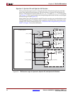
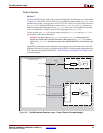
Chapter 6: The Ten-Bit Interface
R
Receiver Logic
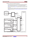
Virtex-II and Virtex-II Pro Devices
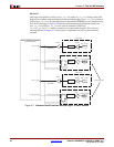
Figure 6-2 illustrates an external receiver TBI in Virtex-II devices. The signal names and
logic displayed precisely match those delivered with the example design when the TBI is
chosen.
Figure 6-2 shows that the input receiver signals are registered in device IOB Double-Data
Rate (DDR) input registers, alternatively on the rising edges of both pma_rx_clk0_bufg
and pma_rx_clk1_bufg (pma_rx_clk0 and pma_rx_clk1 are 180 degrees out of
phase with each other). This splits the input TBI data bus, rx_code_group[9:0], up into
two buses: rx_code_group0_reg[9:0] and rx_code_group1_reg[9:0],
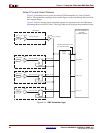
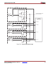
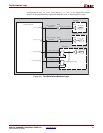
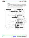
Figure 6-1: Ten-Bit Interface Transmitter Logic
IPAD
IBUFG
IOB LOGIC
gtx_clk
gtx_clk_ibufg
(125 MHz)
BUFG
gtx_clk_bufg
pma_tx_clk
OBUF
FDDRRSE
IOB LOGIC
OPAD
DQ
DQ
pma_tx_clk_obuf
'0'
'1'
DQ
tx_code_group[0]
OBUF
OPAD
tx_code_group_reg[0]
DQ
tx_code_group[9]
OBUF
OPAD
tx_code_group_reg[9]
Ethernet 1000BASE-X PCS/PMA
or SGMII LogiCORE
tx_code_group_int[0]
tx_code_group_int[9]
gtx_clk
tx_code_group[0]
tx_code_group[9]
component_name
_block (Block Level from example design)