


Ethernet 1000BASE-X PCS/PMA or SGMII v9.1 www.xilinx.com 69
UG155 March 24, 2008
R
Chapter 6
The Ten-Bit Interface
This chapter provides general guidelines for creating 1000BASE-X, SGMII or Dynamic
Standards Switching designs using the Ten-Bit Interface (TBI). An explanation of the TBI
logic in all supported device families is provided, as well as examples in which multiple
instantiations of the core are required. Whenever possible, clock sharing should occur to
save device resources.
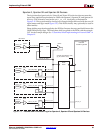
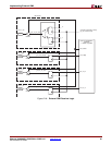
Ten-Bit-Interface Logic
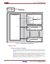
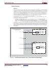
The example design delivered with the core is split between two hierarchical layers, as
illustrated in Figure 4-2. The block level is designed so that it can be instantiated directly
into customer designs and provides the following functionality:
• Instantiates the core from HDL
• Connects the physical-side interface of the core to device IOBs, creating an external
TBI
The TBI logic implemented in the block level is illustrated in all the figures in this chapter.
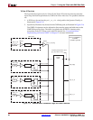
Transmitter Logic
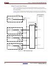
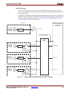
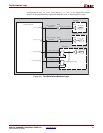
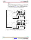
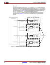
Figure 6-1 illustrates the use of the physical transmitter interface of the core to create an
external TBI in a Virtex-II family device. The signal names and logic shown exactly match
those delivered with the example design when TBI is chosen. If other families are chosen,
equivalent primitives and logic specific to that family will automatically be used in the
example design.
Figure 6-1 shows that the output transmitter data path signals are registered in device IOBs
before driving them to the device pads. The logic required to forward the transmitter clock
is also shown. The logic uses an IOB output Double-Data-Rate (DDR) register so that the
clock signal produced incurs exactly the same delay as the data and control signals. This
clock signal, pma_tx_clk, is inverted with respect to gtx_clk so that the rising edge of
pma_tx_clk occurs in the center of the data valid window to maximize setup and hold
times across the interface.