


Ethernet 1000BASE-X PCS/PMA or SGMII v9.1 www.xilinx.com 77
UG155 March 24, 2008
Clock Sharing across Multiple Cores with TBI
R
Clock Sharing across Multiple Cores with TBI
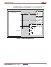
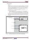
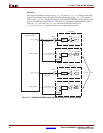
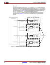
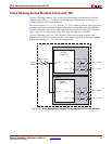
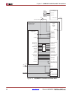
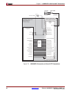
Figure 6-8 illustrates sharing clock resources across multiple instantiations of the core
when using the TBI. gtx_clk may be shared between multiple cores, resulting in a
common clock domain across the device.
The receiver clocks pma_rx_clk0 and pma_rx_clk1 cannot be shared. Each core will be
provided with its own versions of these clocks from its externally connected SERDES.
Figure 6-8 illustrates the receiver clock logic used for the Virtex-II family. See “Receiver
Logic,” page 70, for a description of the clock logic for other device families.
Figure 6-8 illustrates only two cores. However, more can be added using the same
principle. This is done by instantiating the cores using the block level (from the example
design) and sharing gtx_clk across all instantiations.
Figure 6-8: Clock Management, Multiple Core Instances with Ten-Bit Interface
Block Level
IBUFGBUFG
pma_rx_clk0#1
Ethernet 1000BASE-X
PCS/PMA
or SGMII Core
pma_rx_clk0
IBUFGBUFG
pma_rx_clk1#1
pma_rx_clk1
Customer Design
gtx_clk
IBUFGBUFG
pma_rx_clk0#2
Ethernet 1000BASE-X
PCS/PMA
or SGMII Core
pma_rx_clk0
IBUFGBUFG
pma_rx_clk1#2
pma_rx_clk1
gtx_clk
BUFG
IBUFG
gtx_clk
(125MHz)
Block Level