


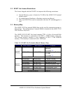
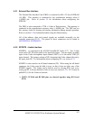
3.4 Using the SDRAM Interface
In order to use the 4M x 32 bits (16 MB) of SDRAM memory, the three SDRAM
control registers must be initialized. The following table shows the standard
configuration for these registers when using the EZ-KIT Lite in the default
configuration. These numbers were derived using the M48LC4M16ATG-75 with
a system clock frequency of 120 MHz.
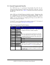
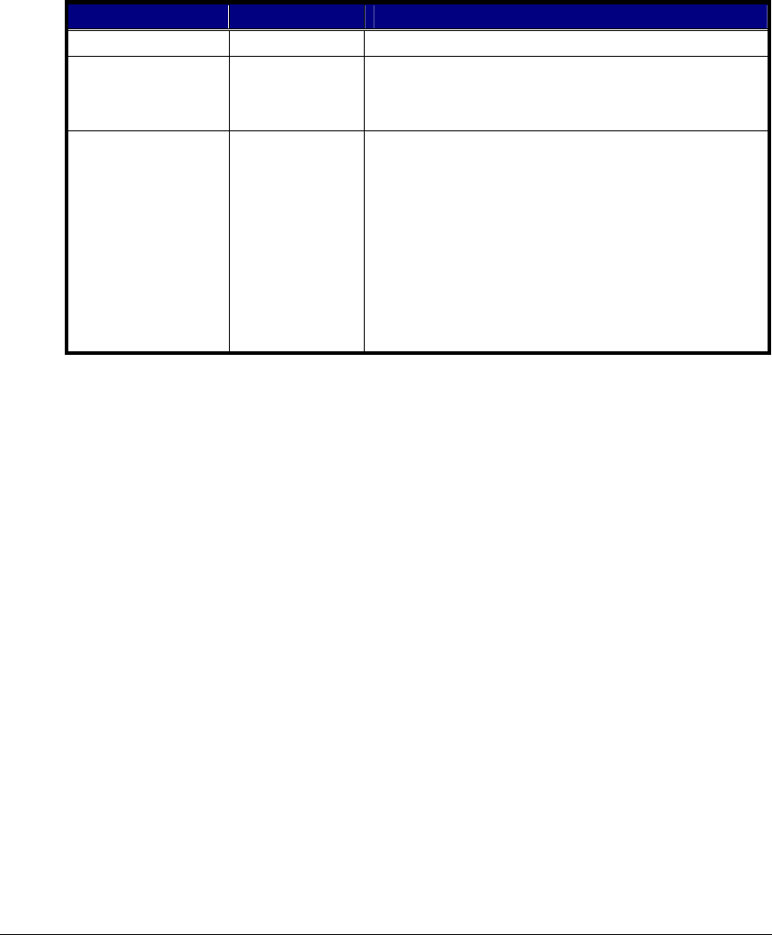
Table 3-2: SDRAM Default Settings
Register Value Function
EBIU_SDRRC 0x0000074A RDIV = 1866 clock cycles
EBIU_SDBCTL 0x00000001 Bank 0 enabled
Bank 0 size = 16 MB
Bank 0 column address width = 8 bits
EBIU_SDGCTL 0x0091998F 32 bit data path
External buffering timing disabled
t
WR
= 2 SCLK cycles
t
RCD
= 3 SCLK cycles
t
RP
= 3 SCLK cycles
t
RAS
= 6 SCLK cycles
pre-fetch disabled
CAS latency = 3 SCLK cycles
SCLK1 disabled
If you are in an EZ-KIT Lite session (that is, not using an emulator), the SDRAM
registers are configured automatically through the debugger. The debugger uses
the values in Table 3-2 whenever bank 0 is accessed through the debugger (such
as viewing memory windows or loading a program). Clearing the appropriate
checkbox on the Target Options dialog box, which is accessible through the
Settings pull-down menu, disables this feature and allows manual configuration.
An example program is included in the EZ-KIT installation directory, which
demonstrates how to setup the SDRAM interface.
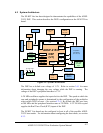
3.5 Using Flash Memory
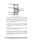
The DSM2150 Flash/PLD chip provides a total of 272K x 16 bits of external flash
memory, arranged into two independent flash arrays (boot and main). The chip
also has a series of configuration registers to control I/O and PLD. This chip is
initially configured with the memory sectors mapped to the DSP as shown below
in Figure 3-1.
ADSP-21535 EZ-KIT Lite Evaluation System Manual
3-3