


Intel® 41110 Serial to Parallel PCI Bridge Design Guide 21
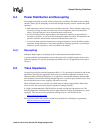
41110 Reset and Power Timing
Considerations 5
This chapter describes the 41110 reset timing considerations.
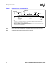
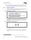
5.1 A_RST# and PERST# Timing Requirements
The PCI-X Specification requires that there is a 100ms delay from valid power (PERST#) to reset
deassertion (A_RST#). 41110 will keep A_RST# asserted for a minimum of 320ms after PERST#
is deasserted.
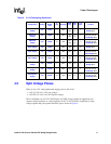
5.2 VCC15 and VCC33 Voltage Requirements
The following steps are the power sequencing requirements that must be followed with the
41110:
1. The 41110 requires that the VCC33 voltage rail be no less than 0.5V below VCC15 (absolute
voltage value) at all times during 41110 operation, including during system power up and
power down. In other words, the following must always be true:
VCC33 >= (VCC15 – 0.5V)
This can be accomplished by placing a diode (with a voltage drop <0.5V) between VCC15 and
VCC33. A node will be connected to VCC15 and cathode will be connected to VCC33.
If VCC15 (1.5V PCI-X I/O voltage) and VCC15 (1.5V core voltage) are tied together on the
platform, then both voltages must meet the above rule.
Note: Linear voltage regulators are recommended when using 1.5 Volt power supplies.
2. If a voltage regulator solution is used which shunts VCC15 to ground while VCC33 is
powered, the maximum allowable time that VCC15 can be shunted to ground while VCC33 is
fully powered is 20ms.
3. The maximum allowed time between VCC33 and VCC15 ramping is 525ms.
Note: There is no minimum sequencing time requirement other than requirements in Steps 2 and 3.