


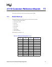
Intel® 41110 Serial to Parallel PCI Bridge Design Guide 47
Circuit Implementations
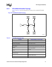
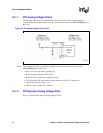
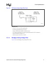
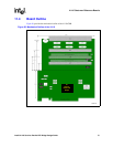
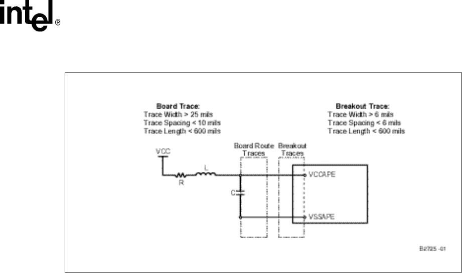
Figure 23. PCI Express Analog Voltage Filter Circuit
Additional Notes:
• Place C as close as possible to package pin.
• R must be placed between VCC15 and L.
• Route VCCAPE and VSSAPE as differential traces.
• VCCAPE and VSSAPE traces must be ground referenced (No VCC15 references).
• Max total board trace length = 1.2”.
• Min trace space to other nets = 30 mils.
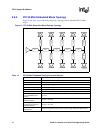
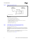
10.1.3 Bandgap Analog Voltage Filter
Figure 24 shows the Bandgap Analog Voltage Filter Circuit.
Serial to
Parallel PCI
Bridge