


Intel® 41110 Serial to Parallel PCI Bridge Design Guide 55
Design Guide Checklist 12
This checklist highlights design considerations that should be reviewed prior to manufacturing an
adapter card that implements the 41110 product. The items contained within this checklist attempt
to address important connections to these devices and any critical supporting circuitry. This is not a
complete list and does not guarantee that a design will function properly.
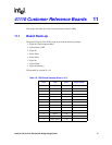
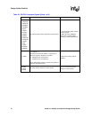
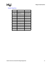
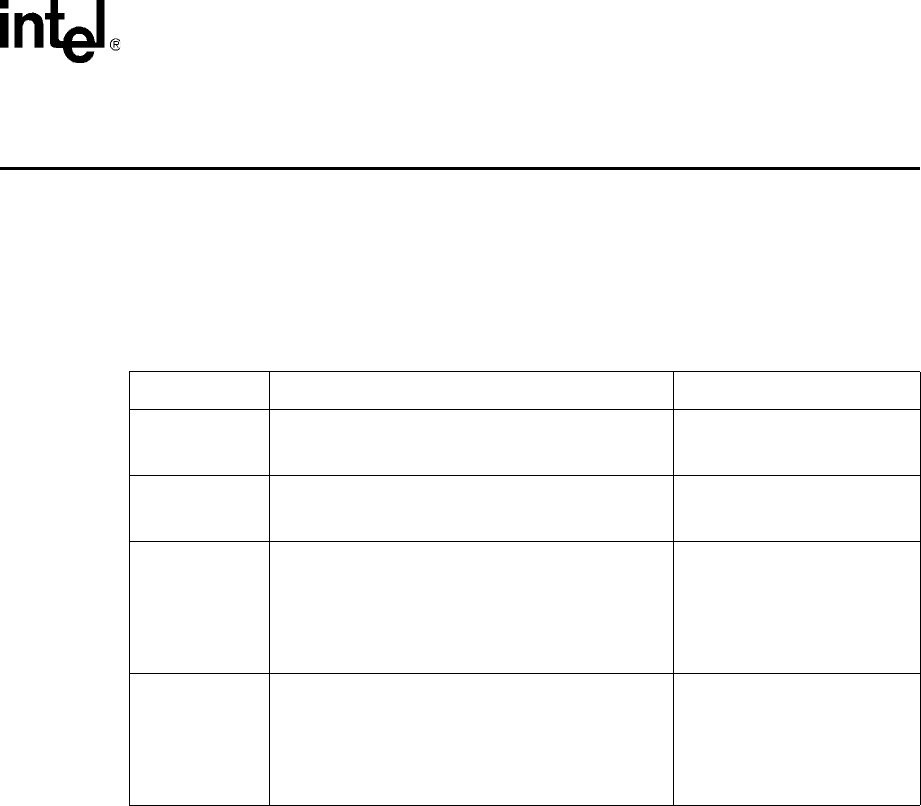
Table 19. PCI Express Interface Signals
Signals Recommendations Reason/Impact
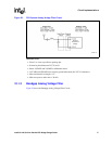
REFCLKn,
REFCLKp
Must be connected to clock from a PCI Express
connector for add-in card designs or to a 100MHz
oscillator for an embedded design.
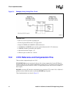
PE_RCOMP[1:0]
24.9Ω ±1% pullup resistor to 1.5V. A single resistor can
be used for both signals. Place resistor as close as
possible to REFCLKn, REFCLKp pins.
PCI Express compensation pin.
0.5V nominal.
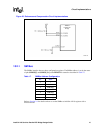
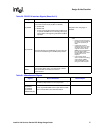
PERP[7:0]
PERN[7:0]
For X1 mode, only signals PERp[0] and PERn[0] or
PERp[7] and PERn[7] are used.
For X4 mode, only signals PERp[3:0] and PERn[3:0]
are used.
For X8 mode, all of these signals, PERp[7:0] and
PERn[7:0], are used.
PCI Express data serial inputs
(differential data receive
signals).
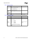
PETP[7:0]
PETN[7:0]
For X1 mode, only signals PETp[0] and PETn[0] or
PETp[7] and PETn[7] are used.
For X4 mode, only signals PETP[3:0] and PETN[3:0]
are used.
For X8 mode, all of these signals, PETP[7:0] and
PETN[7:0], are used.
PCI Express data serial inputs
(differential data transmit
signals).