Intel® 41110 Serial to Parallel PCI Bridge Design Guide 41
PCI Express Layout 9
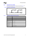
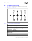
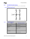
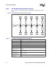
This section provides an overview of the PCI-Express stackup recommended based on Intel
presimulation results. For additional information, refer to the Intel® 41110 Serial to Parallel PCI
Bridge Developer’s Manual or the PCI Express Specification, Revision 1.0 from the
www.pcisig.com
website.
9.1 General recommendations
PCI Express is a serial differential low-voltage point-to-point interconnect. The PCI Express was
designed to support 20 inches between components with standard FR4. The 41110 supports x8 lanes.
PCI-Express requires special considerations be made for interconnect losses, jitter, crosstalk and
mode conversions. The below list provides some general guidelines for the layout of a PCI-Express
trace:
1. Jitter: Trace lengths of a PCB trace can introduce around 1 to 5 ps of jitter and 0.35 to 0.5 dB
of loss per inch of differential pair. An add-in card the trace length from edge-finger pad to
device is limited to 3 inches.
2. Matching within pair: Trace lengths of matching differential pairs are required to be matched
within +/-5 mil delta. Each net within a differential pair should be length matched on a
segment-by-segment basis at point of discontinuity such as an breakout area, routes between
vias, routes between AC coupling capacitors and connector pins.
3. Trace Symmetry: Trace Symmetry is required between two traces of the same differential pair.
4. Vias: Vias contribute 0.5 to 1.0 dB/via toward the loss budget. Vias on an add-in card should
be limited to one near the breakout section of the pads and one near the edge finger.
5. Bends: Trace bends should be kept to a minimum. If bends are used they should be at a 45-
degree angle or smaller. The number of left and right bends should be matched as closely as
possible to even out the overall lengths of each segment of the differential pair.
6. AC Coupling capacitors: AC coupling capacitor with a value of 75nF to 200nF should line
up at the same location from one trace to the other within the pair. The 0402 size capacitor
with a small pad size is highly recommended. The breakout from the capacitor should be
symmetrical for both signal traces in the differential pair.
7. Connector pins: Length compensation for the connector pins of the differential pair being
offset from each other the PCB trace should be considered.
8. Ground Plane Referencing: Ground plane referencing is required along the entire route of the
differential pair. Traces routed near the edge should maintain a 40 mil air gap to the edge.
Layer switching should also maintain the ground plane. Grounds between planes should be
connected with stitching vias (with one to three recommended per differential pair).
9. Breakout Areas: Breakout areas near a device package should be limited to 500 mils in lengths.
The necking down to a smaller trace width should be symmetrical on the differential pair.


