


Intel® 41110 Serial to Parallel PCI Bridge Design Guide 27
Board Layout Guidelines 7
This chapter provides details on adapter card stackup suggestions. It is highly recommended that
signal integrity simulations be run to verify each 41110 PCB layout especially if it deviates from
the recommendations listed in these design guidelines.
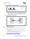
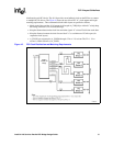
7.1 Adapter Card Topology
The 41110 will be implemented on PCI-E adapter cards with an eight layer stackup PCB. The
specified impedance range for all adapter card implementations will be 60
Ω +/-15%. Adjustments
will be made for interfaces specified at other impedances. Table 3 defines the typical layer
geometries for eight layer boards.
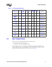
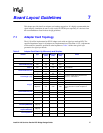
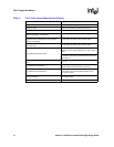
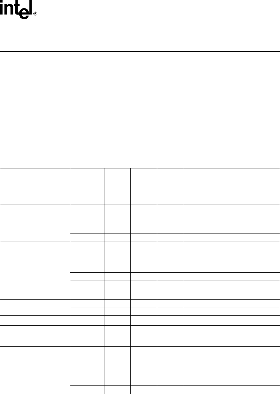
Table 3. Adapter Card Stack Up, Microstrip and Stripline
Variable Type
Nominal
(mils)
Minimum
(mils)
Maximum
(mils)
Notes
Solder Mask Thickness (mil) N/A 0.8 0.6 1.0
Solder Mask E
r
N/A 3.65 3.65 3.65
Core Thickness (mil) N/A 2.8 3.0 3.2
Core E
r
N/A 4.3 3.75 4.85 2113 material
Plane Thickness (mil)
Power 2.7 2.5 2.9
Ground 1.35 1.15 1.55
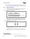
Trace Height
(mil)
13.53.33.7
The trace height will be determined to
achieve a nominal 60 Ω.
23.53.33.7
3 10.5 9.9 11.1
Preg E
r
Microstrip 4.30 3.75 4.85 2113 material
Stripline1 4.30 3.75 4.85 2113 material
Stripline2 4.3 3.75 4.85
7628 material. Trace height 3 is composed
of one piece of 2113 and one piece of
7628.
Trace Thickness (mil)
Microstrip 1.75 1.2 2.3
Stripline 1.4 1.2 1.6
Trace Width (mil) Microstrip 4.0 2.5 5.5
Stripline 4.0 2.5 5.5
Total Thickness (mil) FR4 62.0 56.0 68.0
Trace Spacing (using
microstrip E2E/C2C)
[12]/[16]
Trace Spacing (using
stripline E2E/C2C)
[12]/[16]
Trace Impedance
Microstrip 60 51 69
Stripline 60 51 69