


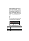
40
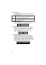
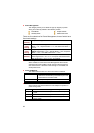
50ns DRAM Timing Type
60ns DRAM Timing Type
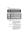
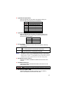
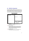
EDO CASx# MA Wait State:
You could select the timing control type of EDO DRAM CAS MA
(memory address bus). The available choices are 1, 2.
EDO RASx# Wait State:
You could select the timing control type of EDO DRAM RAS MA
(memory address bus). The available choices are 1, 2.
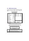
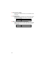
SDRAM RAS to CAS Delay:
You can select RAS to CAS Delay time in HCLKs of 2/2 or 3/3.
The system board designer should set the values in this field,
depending on the DRAM installed. Do not change the values in
this field unless you change specifications of the installed DRAM
or the installed CPU. The available choices are 2, 3.
SDRAM RAS Precharge Time:
Defines the length of time for Row Address Strobe is allowed to
precharge. The available choices are 2, 3.
SDRAM CAS Latency Time:
You can select CAS latency time in HCLKs of 2/2 or 3/3. The
system board designer should set the values in this field,
depending on the DRAM installed. Do not change the values in
this field unless you change specifications of the installed DRAM
or the installed CPU. The available choices are 2, 3.
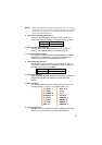
SDRAM Precharge Control:
When enabled, all CPU cycles to SDRAM results in an All Banks
Precharge Command on the SDRAM Interface.
DRAM Data Integrity Mode:
Select Parity or ECC (error-correcting code), according to the type
of installed DRAM. The available choices are Non-ECC, ECC.
System BIOS Cacheable:
Select Enabled allows caching of the system BIOS ROM at
F000h-FFFFFh, resulting in better system performance.
However, if any program writes to this memory area, a system
error may result.
Enabled BIOS access cached
Disabled BIOS access not cached
Video BIOS Cacheable:
Select Enabled allows caching of the video BIOS ROM at
C0000h-F7FFFh, resulting in better video performance. However,
if any program writes to this memory area, a system error may
result.