KS152JB Universal Communications Controller
Technical Specifications
Kawasaki LSI USA, Inc. Page 23 of 120 Ver. 0.9 KS152JB2
The DMA circuitry stops operation in both Idle and power Down modes. Since operation is
stopped in both modes, the process should be similar in each case. Specific steps that need to be
taken include: notification to other devices that DMA operation is about to cease for a particular
station or network, proper withdrawal from DMA operation, and saving the status of the DMA
channels. Again, the status of the I/O pins during Power Down needs careful consideration to
avoid damage to the C152 or other components.
Port 4 returns to its input state, which is high level using weak pullup devices.
2.10 Local Serial Channel
Local Serial port is a full duplex port. This means that it can simultaneously transmit and receive
data. In addition, the receive register is double buffered. This allows reception of the second data
byte before the first byte is read from the receive register. The transmit register and the receive
buffer are both addressed as SBUF Special Function Register. However any write to SBUF will be
to the transmit register, while a read from SBUF will be from the receive buffer register.
The serial port can operate in four different modes.
MODE 0
This mode provides the synchronous communication with external devices. In mode 0, serial data
is transmitted and received on the RXD line. TXD is used to transmit the shift clock. This mode is
therefore a half duplex mode of serial communication. 8 bits are transmitted or received per
frame. The LSB is transmitted/received first. The baud rate is fixed at 1/12 of the oscillator fre-
quency.
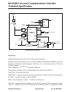
Mode 0 is used to transmit data synchronously, in a half duplex format. The functional block dia-
gram is shown below. Data enters and leaves the Serial port on the RxD line. The Txd line is used
to output the shift clock. The shift clock is used to shift data into and out of the TBO and the
device at the other end of the line.
Any instruction that causes a write to SBUF will start the transmission. The shift clock will get
activated and data will be shifted out on RxD pin til all 8 bits are transmitted. The clock on TxD
then remains low for 6 clock periods and then goes high again. This ensures that at the receiving
end the data on RxD line can be clocked in either on the rising edge of the shift clock on TxD or
latched when the TxD clock is low. The TI flag is set high in S1 following the end of transmission
of the last bit.
The Serial port will receive data when REN is 1 and RI is zero. The shift clock (TxD) will be acti
vated and the serial port will latch data sampled at S5P2 at the rising edge of shift clock. The
external device should therefore present data on the falling edge on the shift clock. This process
continues till all the 8 bits have been received. The RI flag is set in S1 following the last rising
edge of the shift clock on TxD. This will stop reception, till the RI is cleared by software.


