KS152JB Universal Communications Controller
Technical Specifications
Kawasaki LSI USA, Inc. Page 24 of 120 Ver. 0.9 KS152JB2
MODE 1
In Mode 1, the full duplex mode is used. Serial communication frames are made up of 10 bits
transmitted on TXD and received on RXD. The 10 bits consist of a start bit (0), 8 data bits (LSB
first), and a stop bit (1). On receive, the stop bit goes into RB8 in the SFR SCON. The baud rate in
this mode is variable.In this mode 10 bits are transmitted (on TxD) or received (on RxD). The
frame consists of a start bit (0), 8 data bits (LSB first), and a stop bit (1). On reception, the stop bit
is placed into RB8. Tthe baud rate is determined by the Timer 1 or timer 2 overflow rate, and so it
can be controlled by the user.
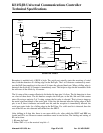
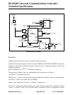
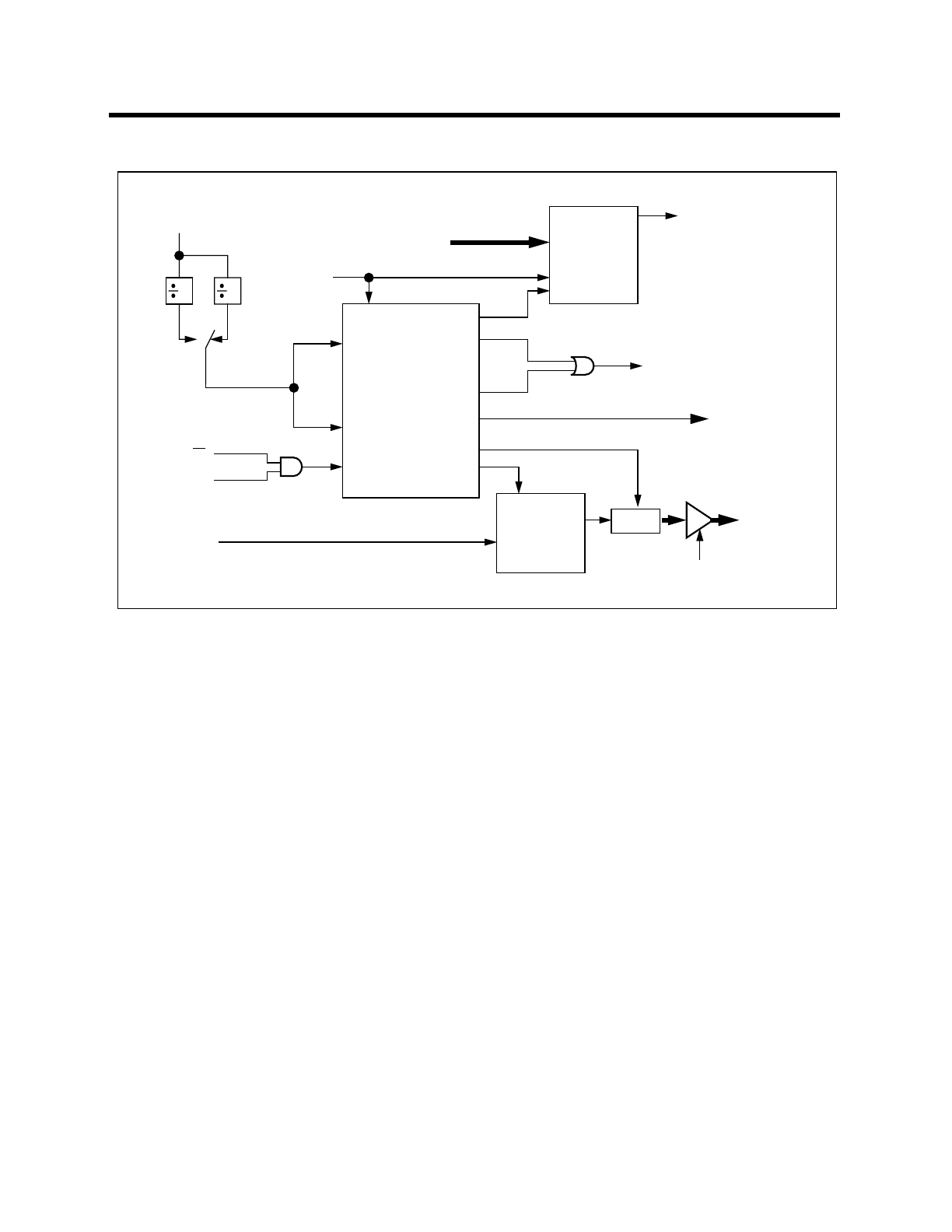
The figure below gives the simplified functional block for Mode 1.
Transmission begins with a write to SBUF. The serial data is brought out on to TxD pin following
the first roll-over of divide by 16 counter. The next bit is placed on TxD pin following the next
rollover of the divide by 16 counter. Thus the transmission is synchronized to the divide by 16
counter and not directly to the write to SBUF signal. After all 8 bits of data are transmitted, the
stop bit is transmitted. The TI flag is set in the S1 state after the stop bit has been put out on TxD
pin. This will be at the 10th rollover of the divide by 16 counter after a write to SBUF.
SOUT
PARIN
LOAD
CLOCK
TX START
TX CLOCK
Transmit Shift Register
SIN
PAROUT
CLOCK
RX CLOCK
RX SHIFT
RX
SBUF
LOAD
SBUF
START
Read
SBUF
TX SHIFT
TI
RI
SERIAL
CONTROLLER
Write to
SBUF
Internal
Data Bus
Internal
Data Bus
RxD
RxD
Serial Interrupt
Receive Shift Register
RI
REN
12 4
SM2
01
P3.0 Alternate
Output function
P3.0 Alternate
Input function
CLOCK
SHIFT
CLOCK
TxD
P3.1 Alternate
Output function
Local Serial Port Mode 0


