


KS152JB Universal Communications Controller
Technical Specifications
Kawasaki LSI USA, Inc. Page 6 of 120 Ver. 0.9 KS152JB2
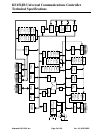
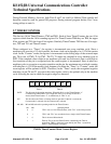
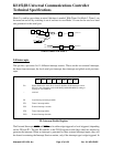
2.2 Special function Registers
The following table lists the SFR’s present in 80152. Note that not all the addresses are occupied
by SFR’s. The unoccupied addresses are not implemented and should not be used by the cus-
tomer. Read access from these unoccupied locations will return unpredictable data, while write
accesses will have no effect on the chip
Note: SFR’s in marked column are bit addressable.
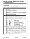
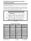
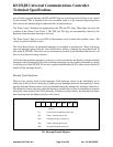
2.3 RESET
The RST pin is the input to a Schmitt Trigger whose output is used to generate the internal system
reset. In order to obtain a reset, the RST pin must be held low for at least four machine cycles,
while the oscillator is running. The CPU internal reset timings are shown in the Figure.
The external reset input RST is sampled on S5P2 in every machine cycle. If the sampled value is
high, then the processor responds with an internal reset signal at S3P1, two machine cycles after
the RST being sampled low. This means that there is an internal delay of 19 to 31 clock periods
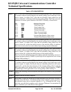
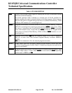
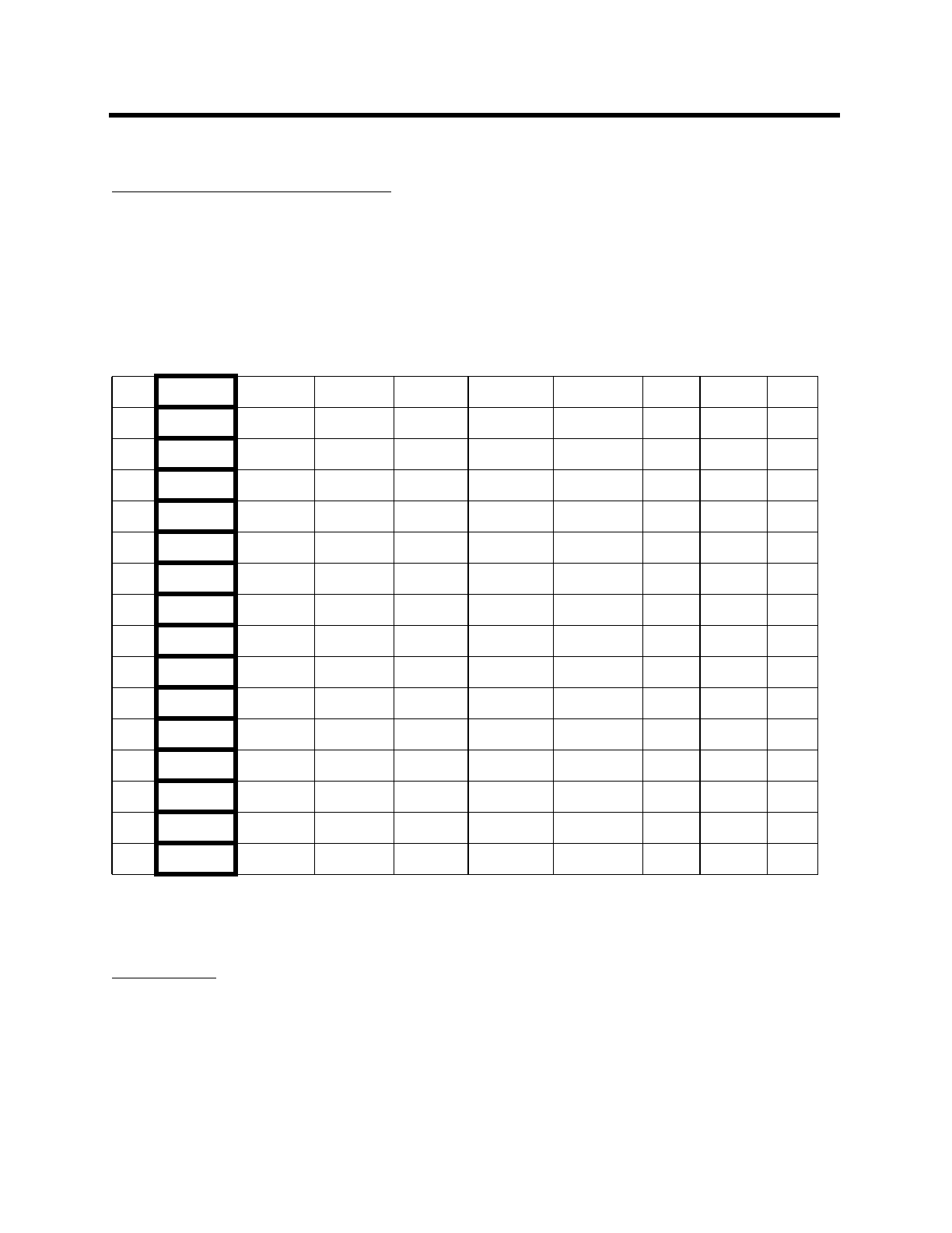
Table 2: SFR map for the cpu
F8 IPN1 FF
F0 B BCRL1 BCRH1 RFIFO MYSLOT F7
E8 RSTAT EF
E0 ACC BCRL0 BCRH0 PBRS AMSK1 E7
D8 TSTAT DF
D0 PSW DARL1 DARH1 TCDCNT AMSK0 D7
C8 IEN1 CF
C0 P4 DARL0 DARH0 BKOFF ADR3 C7
B8 IP BF
B0 P3 SARL1 SARH1 SLOTTM ADR2 B7
A8 IE AF
A0 P2 P6 SARL0 SARH0 IFS ADR1 A7
98 SCON SBUF 9F
90 P1 P5 DCON0 DCON1 BAUD ADR0 97
88 TCON TMOD TL0 TL1 TH0 TH1 8F
80 P0 SP DPL DPH GMOD TFIFO PCON 87