


USER’S GUIDE
050396 106/173
107
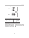
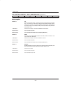
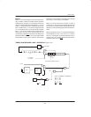
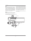
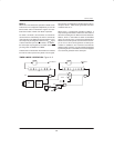
Mode 0
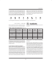
Figure 13–3 is a block diagram of a timer/counter oper-
ating in Mode 0. Mode 0 configures either program-
mable timer for operation as a 13–bit timer/counter. For
Timer 0, selection of Mode 0 configures bit 4 – 0 of TL0
as bits 4 – 0 respectively of the 13–bit timer/counter reg-
ister. In addition, bits 7 – 0 of TH0 are configured as bits
12 – 5 respectively of the 13–bit timer/counter register.
Bits 7 – 5 of TL0 are indeterminate and should be ig-
nored when read. All of the timer/counter bits are
cleared to 0 by a hardware reset. When the TR0 bit is set
with either GATE=0 or INT0
=1, the 13–bit register will be
incremented as each count is received. The previous
value of the 13–bit register is unchanged when the TR0
bit is set to a 1 from a previous 0 condition.
When the 13–bit timer/counter reaches a value of
1FFFH (all 1’s) the next count received will cause the
value to roll over to 0000 and the TF0 flag will be set. Ad-
ditionally, an interrupt will be generated if it had been en-
abled.
Mode 0 operation for Timer 1 is functionally identical to
that described for Timer 0. TH1 and TL1 are used to
form the 13–bit register as just described for Timer 0.
Likewise, TR1, TF1, and INT1 perform the functions de-
scribed for TR0, TF0, and INT0
.
TIMER/COUNTER MODE 0 AND 1 OPERATION Figure 13–3
TF0 INTERRUPT
70
70
1
MUX
MUX
1
INVALID WHEN READ IN MODE 0
0 IF MODE 0
1 IF MODE 1
TH0
TL0
T0 PIN
OSC.
DIVIDE
BY 12
GATE
INT0
PIN
TR0
NOTE: FOR TIMER 1 OPERATION
TF0 ➞ TF1
TH0 ➞ TH1
TL0 ➞ TL1
T0 ➞ T1
TR0 ➞ TR1
INT0
➞ INT1
1 IF C/T = 1
0 IF C/T
= 0
0
0