


USER’S GUIDE
050396 98/173
99
least significant eight bits of address and data. When 1’s
are output on Port 2 for address bits during these cycles,
strong current drivers are employed. The information in
the Port 2 SFR latch is unchanged during these cycles.
Port 0 also employs strong output drivers for 1’s during
these cycles. However, a value of 0FFH will be written to
the Port 0 SFR latch, destroying any previous informa-
tion which was written into it.
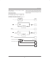
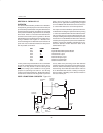
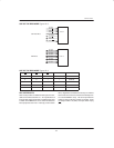
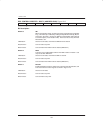
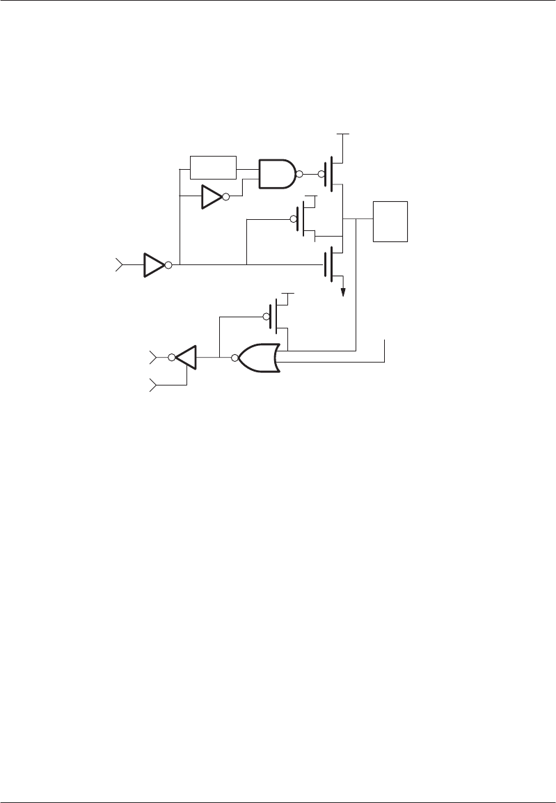
PARALLEL PORT OUTPUT BUFFERS (PORTS 1, 2, AND 3) Figure 12–2
DELAY
= 2Tclk
VCC
VCC
PORT
PIN
POWER
DOWN
VCC
P1
P2
P3
Q FROM
PORT LATCH
INTERNAL
DATA
READ PORT
PIN
INPUT FUNCTION
Any port pin can be used as a general purpose input by
simply writing a logic 1 into the associated SFR latch.
Ports 1, 2, and 3 have weak pull–ups, so they will go to a
logic 1 state. However, the pull–up is sufficiently weak
that an external circuit can easily overdrive it with a logic
0. Thus an output of 1 and an input are the same state.
After setting the latch to a 1, the port can be read. If an
external circuit drives high, reading the port will show
a 1. If the external circuit drives low, the internal pull–up
will be overcome and the pin will be low. Thus the read
operation will see a logic 0. Port 0 is different in that it has
no pull–up. Thus writing a 1 into the Port 0 latch causes
the pin to tri–state. An external pull–up should be used.
In the input state, the external circuit would overdrive the
external pull–up on Port 0.
It can be seen in Figure 12–1 that there are actually two
ways to read a port pin. The CPU can read the latch or
the pin. These need not have identical values. A normal
read instruction will read the state of the pin. It will nei-
ther read, nor modify the state of the latch. For example,
if software writes the latch of Port 1 with an FFh, the port
will output all high values, and also be configured as an
input. If an external circuit pulls down the lower four bits,
a read instruction would see F0h. The latch would still
contain FFh. If the external circuit were to release the
four lower bits, the port would return to the value of FFh.
There are a selected number of instructions that actually
read the latch instead of the pin. These are called Read–
Modify–Write instructions. These instructions read the
state of the latch, possibly modify it, then write the result
back to the latch. The Read–Modify–Write instructions
are listed below.