


USER’S GUIDE
050396 147/173
148
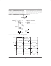
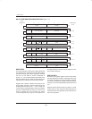
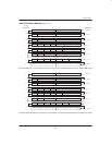
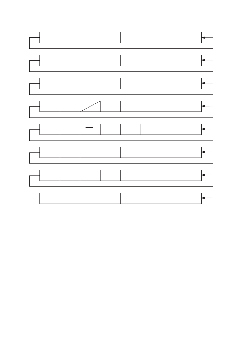
DS1215 TIME REGISTERS DESCRIPTION Figure 17–4
OSC
7 654321 0
0.1 SEC
0
0
HR012/24
0000
00
000
10 YEAR
RANGE (BCD)
00–99
00–59
00–59
01–12
01–07
01–31
01–12
00–99
CLOCK
0
1
2
3
4
5
6
7
REGISTER #
0.01 SEC
10’s OF SECONDS SECONDS
10’s OF MINUTES MINUTES
10
A/P
HOUR
DAY
10 DATE DATE
10
MON
MONTH
YEAR
00–23
REGISTERS
The time information is contained in eight registers that
are each 8 bits long. After the 64–bit recognition pattern
has been received, data in these registers is accessed
one bit at a time which is shown conceptually in
Figure 17–4. It is recommended that data written to the
RTC be handled in groups of 8 bits corresponding to the
register bytes in order to prevent erroneous results.
Register data is always in BCD format except for the
hours register (register 3), whose format changes de-
pending upon the state of bit 7. If bit 7 is high, the
12–hour mode is selected and bit 5 of the hours register
becomes an AM/PM indicator; if bit 7 is low, the 24–hour
mode is selected and bit 5 becomes the second
10–hour bit (20–23 hours). Figure 17–5 contains exam-
ples that illustrate the content of these registers for dif-
ferent modes and times.
SPECIAL BITS
Bit 5 of the days register (register 4) is the control bit for
the clock micropower oscillator. Clearing bit 5 to a logic
0 enables the oscillator for normal operation; setting bit
5 to a logic 1 disables the oscillator and halts the time-
keeping. It is recommended that bit 5 always be cleared
to 0.
Register locations shown as logic 0’s in Figure 17–4 will
always return a 0 when being read. Write operations to
these bit locations are ignored by the clock and have no
effect on its operation.