


USER’S GUIDE
050396 97/173
98
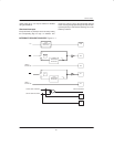
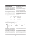
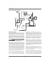
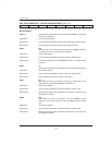
PORT 3 FUNCTIONAL CIRCUITRY
VCC
POWER
DOWN
PORT
3.n
WRITE
ENABLE
READ
ENABLE
READ
LATCH/PIN
DQ
VCC
VCC
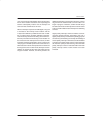
SERIAL I/O AND EXTERNAL
MEMORY CONTROL
RXD, TXD
WR
, RD
INPUTS
INTERNAL
DATA BUS
Q
DELAY
= 2Tclk
SERIAL TIMER AND
INTERRUPT INPUTS
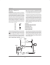
OUTPUT FUNCTIONS
Slightly different output buffer structures are implement-
ed for the four parallel I/O ports. When the pins are used
strictly for parallel I/O, ports 1, 2, and 3 have internal
weak pull–up devices. Port 0, on the other hand, has a
totem–pole output structure. When used as outputs, all
port pins will drive the state to which the associated SFR
latch bit has been set except for Port 0 which will only
drive low. Port 0 requires a pull–up to drive high when
used as parallel I/O. Port 0 functions as true I/O when
used as the multiplexed address/data bus.
When an instruction is executed that writes a new value
to the SFR latch for a parallel I/O port, the write actually
occurs at S6P2 of the final machine cycle of the instruc-
tion. There is an additional delay in that the output buff-
ers only sample the state of the latch’s output during
Phase 1 of any given clock period. As a result, the new
value which is written to the latch will appear on the pin
at S1P1 of the machine cycle following the final cycle of
the instruction which performs the write to the port latch.
See the section on CPU timing for clock details.
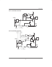
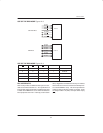
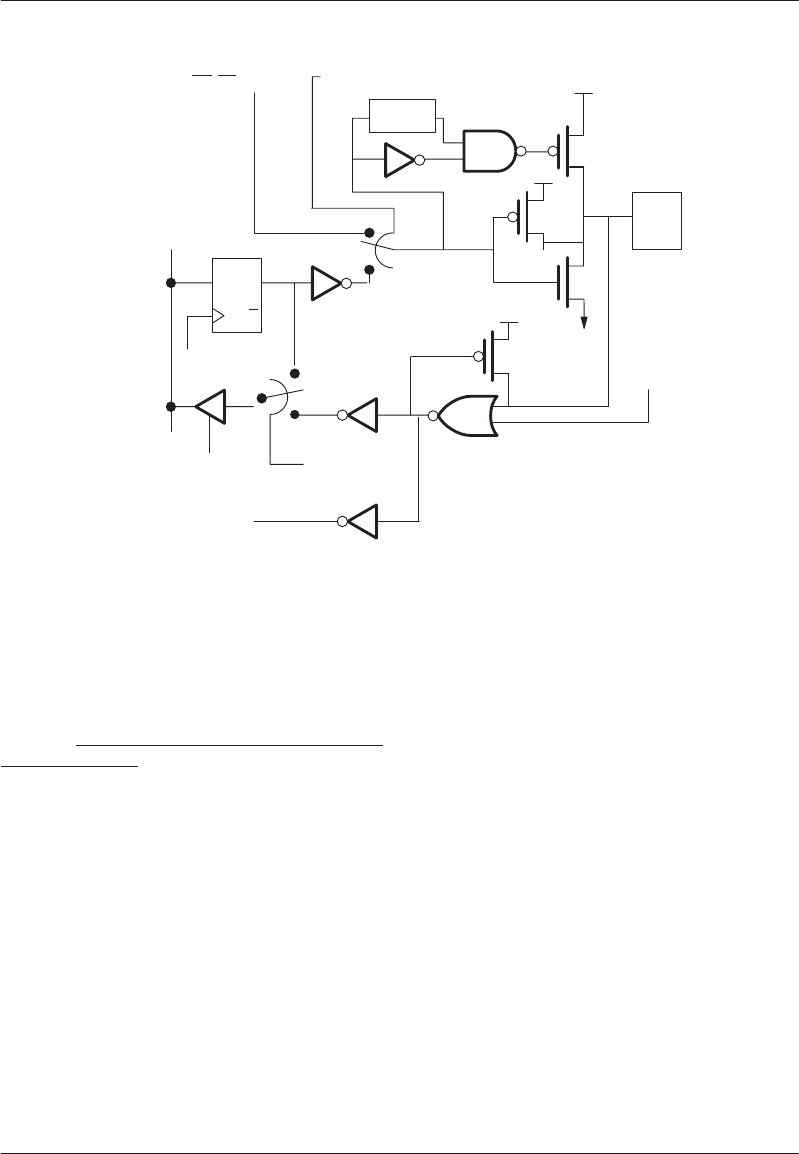
Port 1, 2, and 3 activate additional high–current pull–up
devices when a write operation to the port necessitates
a 0– to–1 transition on the I/O pin in order to speed up
the transition time. The structure of these devices is il-
lustrated in Figure 12–2. The pull–up structure is com-
prised of three pFET devices which are turned on when
a logic 0 is applied to their gates and turned off when a 1
is applied. An n–channel device is used to drive a 0 on
the pin and is turned on and off in the inverse sense of
the pFET. When a 1 is applied, the n–channel FET is
turned on and it is turned off when a 0 is applied.
Following a 0–to–1 change in the state of the latch bit,
transistor P1 will be turned on for two oscillator periods.
This extra pull–up device can source about 10 mA (100
times more current than the normal P3 device). While
P1 is turned on, it will in turn activate P3. The gate and
P3 form a latch when P1 is turned off so that the state will
be maintained on the pin.
P2 is a very weak pull–up device (about 1/10 the
strength of P3) whose sole purpose is to restore a 1 to
the pin should a negative glitch cause a 1 to be lost by
forcing the latch to a 0 state.
When an access on the Expanded bus takes place, the
pins of Port 0 and Port 2 are driven with address/data
information. Port 2 outputs the most significant eight bits
of address while Port 0 is time–multiplexed with the