


© National Instruments Corporation 3-1 NI 6115/6120 User Manual
3
Hardware Overview
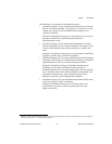
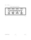
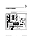
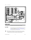
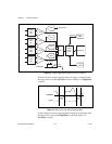
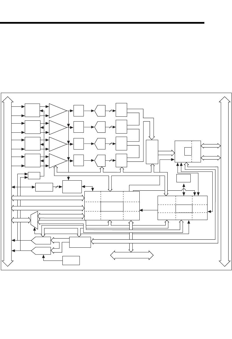
This chapter presents an overview of the hardware functions on the
NI 6115/6120. Figures 3-1 and 3-2 provide block diagrams for the NI 6115
and NI 6120, respectively.
Figure 3-1. NI 6115 Block Diagram
Timing
PFI / Trigger
I/O Connector
RTSI Bus
STC Digital I/O (8)
EEPROM
+
CH0
Amplifier
–
Calibration
Mux
AI CH0
Mux
Analog
Trigger
Circuitry
2
Trigger Level
DACs
Trigger
Calibration
DACs
DAC1
DAQ - STC
Analog Input
Timing/Control
Analog Output
Timing/Control
Digital I/O
Trigger
Counter/
Timing I/O
RTSI Bus
Interface
DMA/IRQ
Bus
Interface
DAC
FIFO
Address/Data
Control
Data (32)
Analog
Input
Control
EEPROM
Control
DMA
Interface
FPGA
DAQ-STC
Bus
Interface
Analog
Output
Control
I/O
Bus
Interface
IRQ
DMA
Mini
MITE
Generic
Bus
Interface
PCI
Bus
Interface
CH0+
CH0–
+
CH1
Amplifier
–
AI CH1
Mux
CH1
Latch
CH1+
CH1–
+
CH2
Amplifier
–
AI CH2
Mux
CH2
Latch
CH2+
CH2–
+
CH3
Amplifier
–
AI CH3
Mux
CH3
Latch
CH3+
CH3–
AI Control
Data (16)
Data (16)
Data (16)
Data (16)
ADC
FIFO
Data (12)
DIO
FIFO
DIO
Control
AO Control
FPGA Digital I/O (8)
Digital I/O (8)
PXI/PCI Bus
DAC0
Anti-
Aliasing
Filter
CH0
12-Bit
ADC
12
Anti-
Aliasing
Filter
CH1
12-Bit
ADC
12
Anti-
Aliasing
Filter
CH2
12-Bit
ADC
12
Anti-
Aliasing
Filter
CH3
12-Bit
ADC
12
DIO
MUX
CH0
Latch
Data (32)